Figure 2–3. jtag chain – Altera Arria V SoC Development Board User Manual
Page 19
Chapter 2: Board Components
2–11
FPGA Configuration
July 2014
Altera Corporation
Reference Manual
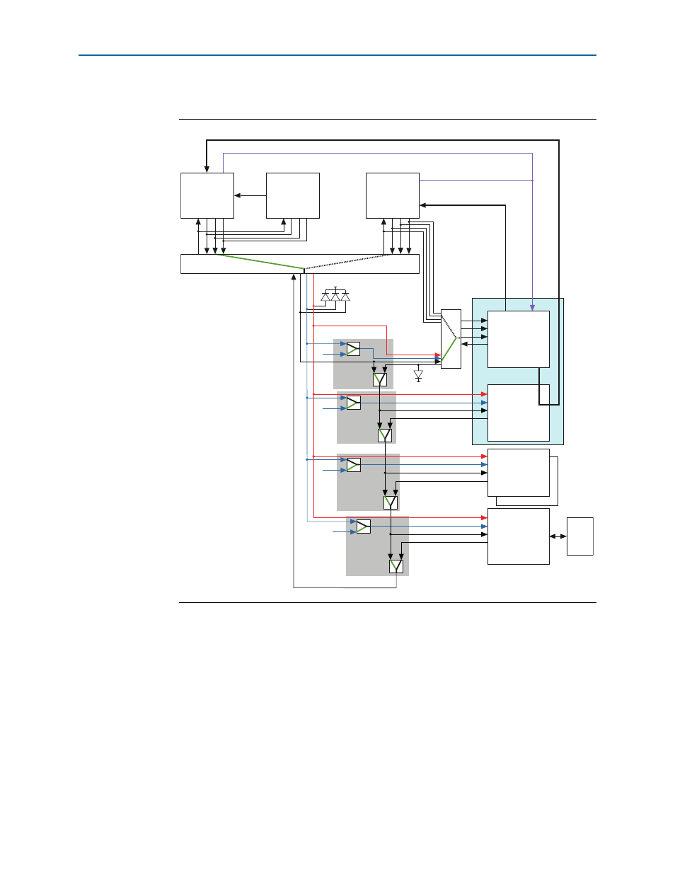
illustrates the JTAG chain.
The JTAG chain control DIP switch (SW4) controls the jumpers shown in
.
To connect a device or interface to the chain, their corresponding switch must be in
the OFF position. Slide all the switches in the ON position to only have the FPGA in
the chain.
1
The MAX V CPLD 5M2210 System Controller must be in the JTAG chain to use some
of the GUI interfaces.
Figure 2–3. JTAG Chain
1
2.5 V
1
1
1
2.5 V
Disable
Trace
Trace
TCK
TMS
TDI
TDO
TRST
Cypress On-Board
USB-Blaster II
TCK
TMS
TDI
TDO
10-Pin
JTAG Header
TCK
TMS
TDI
TDO
TRST
Mictor-38
Header
TCK
TMS
TDI
TDO
TRST
Arria V ST HPS
TCK
TMS
TDI
TDO
TRST
Arria V ST FPGA
FMC Port A
FMC Port B
TCK
TMS
TDI
TDO
MAX V CPLD 5M2210
System Controller
Flash
Memory
TCK
TMS
TDI
TDO