Character lcd, Clock circuitry, On-board oscillators – Altera Arria V SoC Development Board User Manual
Page 29: Character lcd –21, Clock circuitry –21, On-board oscillators –21, Figure 2–5. arria v soc development board clocks
Chapter 2: Board Components
2–21
Clock Circuitry
July 2014
Altera Corporation
Reference Manual
Character LCD
The development board includes a single 10-pin 0.1" pitch single-row header that
interfaces to a 2 line × 16 character Lumex character LCD using standard I
2
C interface
connected to the HPS. The character LCD has a two headers that mount directly to the
board's 10-pin header, so it can be easily removed for access to components under the
display. You can also use the header for debugging, I
2
C expansion, or other purposes.
f
For more information such as timing, character maps, interface guidelines, and other
related documentation, visi
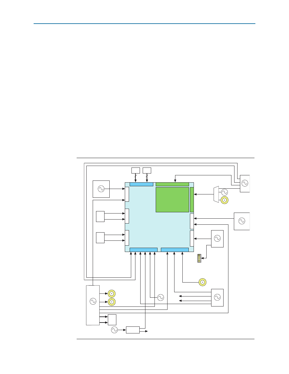
Clock Circuitry
This section describes the board's clock inputs and outputs.
On-Board Oscillators
shows the default frequencies of all external clocks going to the
Arria V SoC development board.
Figure 2–5. Arria V SoC Development Board Clocks
Arria V ST I3
Bank 8
HPS Peripherals
HPS Core
HPS Memor
y Interf
ace
Bank R1
Bank 3
Bank 4
Bank 0L
Bank 1L
Bank 2L
REFCLKL5
Si571
148.5 MHz/I
2
C
REFCLKL3
PCIe
Socket
LMK04828
Cleaner
Si5338
SMA
SMA
SMA
CLK_OSC2
REFCLKR3
REFCLKR2
25 MHz
CLK16-19pFMC
CLK20-23pFMCB
4
4
REFCLKR0
Dual ENET PHY, 25 MHz
MAX V, 100 MHz
CLK0p 100 MHz
CLK1p 156.25 MHz
CLK2p CLK_ENET_PHY 25 MHz
CLK3p 50 MHz
CLK4p CLK_ENET_FPGA 125 MHz
CLK6p CLEAN_CLK
CLK8p SYSREF
CLK10p 100 MHz
CLK11p SMA
SL 18860C
Si570
CLK_OSC1
25 MHz
SMA
Bank R0
FMCA
FMCB
FMCA
REFCLKL2
REFCLKL1
FMCB
REFCLKL0
REFCLKL4
FMCA
FMCB
100 MHz/I
2
C
Si52112
100 MHz
Si5335
125 MHz
125 MHz
MAX V
50 MHz
33 MHz