Altera Arria V SoC Development Board User Manual
Page 17
Chapter 2: Board Components
2–9
MAX V CPLD 5M2210 System Controller
July 2014
Altera Corporation
Reference Manual
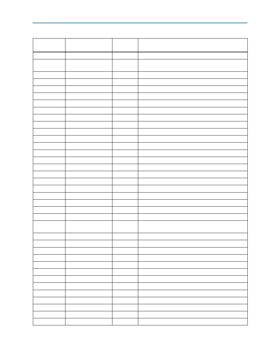
L5
M570_PCIE_JTAG_EN
2.5-V
PCI Express JTAG enable for the on-board USB-Blaster II
H2
MAX_AS_CONF
2.5-V
Driven low to enable AS configuration from the EPCQ flash
through U13 to the FPGA
E11
MAX_CONF_DONE
2.5-V
On-board USB-Blaster II configuration done LED
A4
MAX_ERROR
2.5-V
FPGA configuration error LED
G4
MAX_FPGA_MISO
2.5-V
FPGA to MAX V SPI bus data output
G1
MAX_FPGA_MOSI
2.5-V
FPGA to MAX V SPI bus data input
H3
MAX_FPGA_SCK
2.5-V
FPGA to MAX V SPI bus clock
G5
MAX_FPGA_SSEL
2.5-V
FPGA to MAX V SPI bus slave select
A6
MAX_LOAD
2.5-V
FPGA configuration active LED
K2
MAX_QSPI_RSTN
2.5-V
QSPI reset
M9
MAX_RESETN
2.5-V
MAX V reset push button
B10
MSEL0
2.5-V
FPGA MSEL0 setting
B3
MSEL1
2.5-V
FPGA MSEL1 setting
C10
MSEL2
2.5-V
FPGA MSEL2 setting
C12
MSEL3
2.5-V
FPGA MSEL3 setting
C6
MSEL4
2.5-V
FPGA MSEL4 setting
E10
OVERTEMP
2.5-V
Temperature monitor fan enable
D12
PGM_CONFIG
2.5-V
Load the flash memory image identified by the PGM LEDs
B14
PGM_LED0
2.5-V
Flash memory PGM select indicator 0
C13
PGM_LED1
2.5-V
Flash memory PGM select indicator 1
B16
PGM_LED2
2.5-V
Flash memory PGM select indicator 2
B13
PGM_SEL
2.5-V
Toggles the PGM_LED[2:0] LED sequence
P13
RST
1.5-V
Reset input
R12
SECURITY_MODE
1.5-V
DIP switch for the On-board USB-Blaster II to send FACTORY
command at power up
A10
SI570_EN
2.5-V
Si570 programmable clock enable
D4
SI571_EN
2.5-V
Si571 programmable clock enable
R16
TRST
1.5-V
Reset output
H5
USB_B2_CLK
2.5-V
On-board USB-Blaster II interface clock
R4
USB_CFG0
1.5-V
On-board USB-Blaster II interface (reserved for future use)
T4
USB_CFG1
1.5-V
On-board USB-Blaster II interface (reserved for future use)
P8
USB_CFG2
1.5-V
On-board USB-Blaster II interface (reserved for future use)
T7
USB_CFG3
1.5-V
On-board USB-Blaster II interface (reserved for future use)
N8
USB_CFG4
1.5-V
On-board USB-Blaster II interface (reserved for future use)
R8
USB_CFG5
1.5-V
On-board USB-Blaster II interface (reserved for future use)
T8
USB_CFG6
1.5-V
On-board USB-Blaster II interface (reserved for future use)
T9
USB_CFG7
1.5-V
On-board USB-Blaster II interface (reserved for future use)
R9
USB_CFG8
1.5-V
On-board USB-Blaster II interface (reserved for future use)
Table 2–3. MAX V CPLD System Controller Device Pin-Out (Part 4 of 5)
Board
Reference (U27)
Schematic Signal Name
I/O Standard
Description