Fpga programming from flash memory, Fpga programming from flash memory –13 – Altera Arria V SoC Development Board User Manual
Page 21
Chapter 2: Board Components
2–13
FPGA Configuration
July 2014
Altera Corporation
Reference Manual
FPGA Programming from Flash Memory
Flash memory programming is possible through a variety of methods. The default
method is to use the factory design—Golden Hardware Reference Design. This design
contains an on-board web server, which serves the Board Update Portal (BUP) web
application. The web page allows you to link to SoC-related web pages and to control
some user I/O and LCD on the development board.
On either power-up or by pressing the program configuration push button,
PGM_CONFIG
(S12), the MAX V CPLD 5M2210 System Controller's PFL configures the
FPGA from the flash memory. The PFL megafunction reads 16-bit data from the flash
memory and converts it to fast passive parallel (FPP) format. This 16-bit data is then
written to the dedicated configuration pins in the FPGA during configuration.
Pressing the PGM_CONFIG push button (S12) loads the FPGA with a hardware page
based on which PGM_LED[2:0] (D41, D42, D43) illuminates.
lists the design that loads when you press the PGM_CONFIG push button.
A EPCQ device is used for FPGA configuration in Active Serial (AS) mode on power-
up. The EPCQ device with non-volatile memory features a simple six-pin interface
and a small form factor. The EPCQ supports AS x1 and x4 modes.
By default, this board has a FPP configuration scheme setting. The MAX_AS_CONF pin
needs to be driven from the MAX V CPLD to enable the bus switch to isolate the
EPCQ flash (U28) from the configuration bus. This happens when the MSEL is 10010
or 10011.
B8
FX2_RESETN
K9
3.3-V
On-board USB-Blaster hard reset
F3
FX2_SCL
J4
3.3-V
USB 2.0 PHY serial clock
G3
FX2_SDA
—
3.3-V
USB 2.0 PHY serial data
A1
FX2_SLRDN
K1
3.3-V
Read strobe for slave FIFO
B1
FX2_SLWRN
J9
3.3-V
Write strobe for slave FIFO
B7
FX2_WAKEUP
—
3.3-V
USB 2.0 PHY wake signal
G2
USB_B2_CLK
E2
3.3-V
USB 2.0 PHY 48-MHz interface clock
Table 2–4. USB 2.0 PHY Schematic Signal Names and Functions (Part 2 of 2)
Board Reference
(U61)
Schematic
Signal Name
MAX II CPLD Pin
Number
I/O Standard
Description
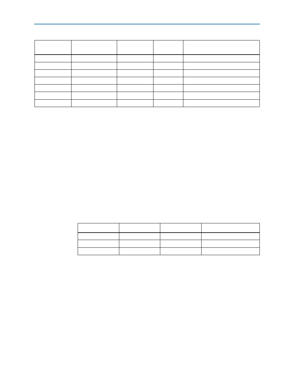
Table 2–5. PGM_LED Settings
PGM_LED0 (D43)
PGM_LED1 (D42)
PGM_LED2 (D41)
Design
ON
OFF
OFF
Factory hardware
OFF
ON
OFF
User hardware 1
OFF
OFF
ON
User hardware 2
Note to
:
(1) ON indicates a setting of ’0’ while OFF indicates a setting of ’1’.