Altera Arria V SoC Development Board User Manual
Page 54
2–46
Chapter 2: Board Components
Memory
July 2014
Altera Corporation
Reference Manual
P8
DDR3_HPS_A4
A8
1.5-V SSTL Class I
Address bus
P2
DDR3_HPS_A5
B7
1.5-V SSTL Class I
Address bus
R8
DDR3_HPS_A6
B9
1.5-V SSTL Class I
Address bus
R2
DDR3_HPS_A7
A9
1.5-V SSTL Class I
Address bus
T8
DDR3_HPS_A8
D9
1.5-V SSTL Class I
Address bus
R3
DDR3_HPS_A9
C10
1.5-V SSTL Class I
Address bus
L7
DDR3_HPS_A10
K7
1.5-V SSTL Class I
Address bus
R7
DDR3_HPS_A11
J7
1.5-V SSTL Class I
Address bus
N7
DDR3_HPS_A12
F9
1.5-V SSTL Class I
Address bus
T3
DDR3_HPS_A13
E9
1.5-V SSTL Class I
Address bus
T7
DDR3_HPS_A14
D11
1.5-V SSTL Class I
Address bus
M2
DDR3_HPS_BA0
L7
1.5-V SSTL Class I
Bank address bus
N8
DDR3_HPS_BA1
C9
1.5-V SSTL Class I
Bank address bus
M3
DDR3_HPS_BA2
D8
1.5-V SSTL Class I
Bank address bus
K3
DDR3_HPS_CASN
G9
1.5-V SSTL Class I
Row address select
K9
DDR3_HPS_CKE
R8
1.5-V SSTL Class I
Column address select
J7
DDR3_HPS_CLK_P
A11
Differential 1.5-V
SSTL Class I
Differential output clock
K7
DDR3_HPS_CLK_N
B10
Differential 1.5-V
SSTL Class I
Differential output clock
L2
DDR3_HPS_CSN
H9
1.5-V SSTL Class I
Chip select
E7
DDR3_HPS_DM4
T7
1.5-V SSTL Class I
Write mask byte lane
E3
DDR3_HPS_DQ32
G1
1.5-V SSTL Class I
Data bus
G2
DDR3_HPS_DQ33
F1
1.5-V SSTL Class I
Data bus
F2
DDR3_HPS_DQ34
P6
1.5-V SSTL Class I
Data bus
F8
DDR3_HPS_DQ35
L1
1.5-V SSTL Class I
Data bus
F7
DDR3_HPS_DQ36
M2
1.5-V SSTL Class I
Data bus
H8
DDR3_HPS_DQ37
M1
1.5-V SSTL Class I
Data bus
H7
DDR3_HPS_DQ38
N1
1.5-V SSTL Class I
Data bus
H3
DDR3_HPS_DQ39
R6
1.5-V SSTL Class I
Data bus
F3
DDR3_HPS_DQS_P4
J1
Differential 1.5-V
SSTL Class I
Data strobe P byte lane 4
G3
DDR3_HPS_DQS_N4
H1
Differential 1.5-V
SSTL Class I
Data strobe N byte lane 4
K1
DDR3_HPS_ODT
H7
1.5-V SSTL Class I
On-die termination enable
J3
DDR3_HPS_RASN
G8
1.5-V SSTL Class I
Row address select
T2
DDR3_HPS_RESETN
E3
1.5-V SSTL Class I
Reset
L3
DDR3_HPS_WEN
J8
1.5-V SSTL Class I
Write enable
L8
DDR3_HPS_ZQ01
—
1.5-V SSTL Class I
ZQ impedance calibration
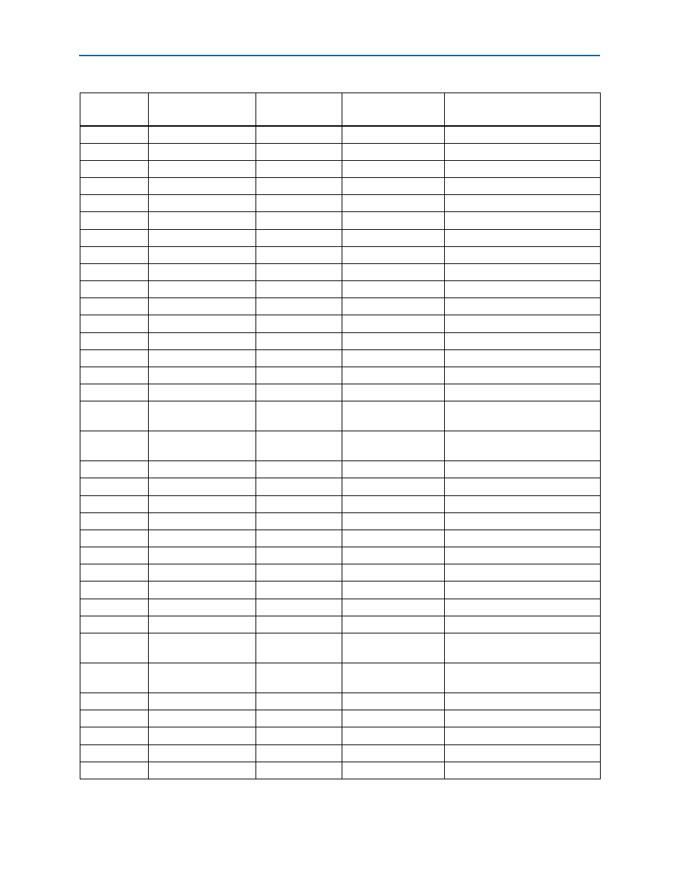
Table 2–28. DDR3 SDRAM Pin Assignments, Schematic Signal Names, and Functions (Part 2 of 5)
Board
Reference
Schematic
Signal Name
Arria V SoC Pin
Number
I/O Standard
Description