Real-time clock (hps), Real-time clock (hps) –37 sfp+ –37 – Altera Arria V SoC Development Board User Manual
Page 45
Chapter 2: Board Components
2–37
Components and Interfaces
July 2014
Altera Corporation
Reference Manual
Real-Time Clock (HPS)
The HPS system has a battery-backed real-time clock (RTC) connected through the I
2
C
interface. The RTC is implemented using a DS1339 device from Maxim
Semiconductor. The device has a built-in power sense circuit that detects power
failures and automatically switches to backup battery supply, maintaining time. The
device uses a CR1225 lithium coin battery with a nominal voltage of 3 V. Using typical
current capacity, the RTC is expected to have 120,000 backup hours. The battery is
mounted inside a holder attached to the board to allow battery replacement or
removal.
lists the RTC device pin assignments, signal names, and functions. The
signal names and types are relative to the Arria V SoC in terms of I/O setting and
direction.
SFP+
The development board include two SFP+ ports that uses two transceiver channels
from the FPGA. These ports takes in serial data from the FPGA and transform them
into optical signals. Both SFP+ ports are active and include the SFP+ cage assembly.
list the SFP+ ports interface pin assignments, signal names, and functions.
18
RESET_HPS_UARTB_N
—
3.3-V
Reset
11
POWER_ENB
—
3.3-V
Power
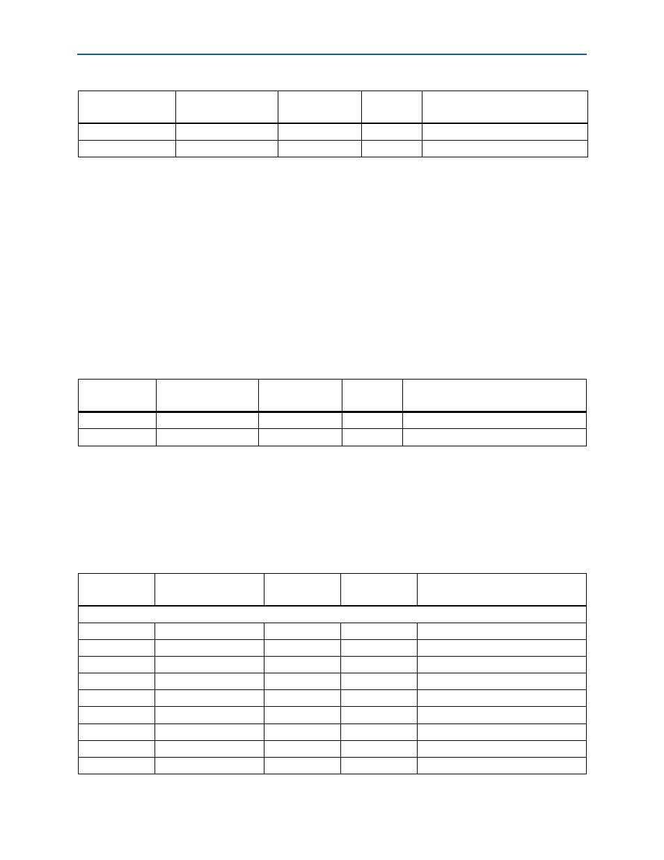
Table 2–23. RS-232 UART Schematic Signal Names and Functions
Board Reference
Schematic Signal
Name
Arria V SoC Pin
Number
I/O Standard
Description
Table 2–24. RTC Device Schematic Signal Names and Functions
Board
Reference (U11)
Schematic Signal
Name
Arria V SoC Pin
Number
I/O Standard
Description
16
I2C_SDA_HPS
C13
3.3-V
Management serial data
1
I2C_SCL_HPS
L13
3.3-V
Management serial clock
Table 2–25. SFP+ Ports Pin Assignments, Schematic Signal Names, and Functions (Part 1 of 2)
Board
Reference
Schematic
Signal Name
Arria V SoC
Pin Number
I/O Standard
Description
SFP+ Port A (J44)
6
SFPA_MOD0_PRSNTn
AR9
3.3-V LVTTL
Module present indicator
8
SFPA_LOS
AV7
3.3-V LVTTL
Signal present indicator
2
SFPA_TXFAULT
AL9
3.3-V LVTTL
Transmitter fault indicator
12
SFPA_RX_N
AE2
PCML
Receiver data
13
SFPA_RX_P
AE1
PCML
Receiver data
5
SFPA_MOD1_SCL
AT8
3.3-V LVTTL
Serial 2-wire clock
4
SFPA_MOD1_SDA
AH8
3.3-V LVTTL
Serial 2-wire data
3
SFPA_TXDISABLE
AP7
3.3-V LVTTL
Drive low to disable transmitter
19
SFPA_TX_N
AD4
PCML
Transmitter data