Altera Hybrid Memory Cube Controller User Manual
Page 66
8. Change directory to <example design directory>
/example_design/par
.
9. Select
hmcc_example.qpf
.
10.Click Processing > Start Compilation. The project compiles and generates a SRAM Object File,
hmcc_
example.sof
, in the
output_files
folder.
11.Prepare the Arria 10 FPGA Development Kit board.
Note: Ensure that power is turned off before you change any settings.
• Add shunts to the J8 jumper to select 1.5V as the V
CCIO
setting for FMC connector B.
• Add shunts to the J11 jumper to select 1.8V as the V
CCIO
setting for FMC connector A.
12.Prepare the HMC mezzannine card.
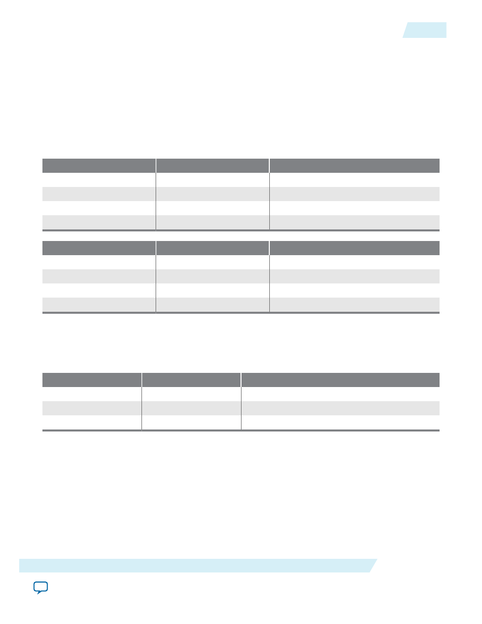
• Set DIP switch SW1 to indicate cube ID 0:
Switch
Function
Setting
1
CUB[0]
Open
2
CUB[1]
Open
3
CUB[2]
Open
4
—
Don't Care
• Set DIP switch SW2 to specify clock settings:
Switch
Function
Setting
1
CLK1_FSEL0
Open (125 MHz)
2
CLK1_FSEL1
Open (125 MHz)
3
CLK1_SEL
Open (Crystal)
4
—
Don't Care
13.Use the Quartus II Programmer to configure the device on the Arria 10 FPGA Development Kit board.
After successful configuration, LED D7 on the board should display a red heartbeat (pulsing).
14.On the board, press user-defined push button PB0 (board reference S3 or schematic signal USER_PB0)
to start the testbench.
The following LEDs on the board indicate testbench results:
LED
Color
Meaning When Lit
D10
Red
Test failed
D9
Green
Test passed
D8
Green
Link initialization completed
Related Information
•
For information about the Altera development kit that the example designs targets.
•
For information about programming an Altera device, refer to the "Quartus II Programmer" chapter.
UG-01152
2015.05.04
HMC Controller IP Core Example Design
6-3
HMC Controller IP Core Example Design
Altera Corporation