Power supply, Power supply –45 – Altera Cyclone V GX FPGA Development Board User Manual
Page 53
Chapter 2: Board Components
2–45
Power Supply
May 2013
Altera Corporation
Cyclone V GX FPGA Development Board
Reference Manual
Power Supply
You can power up the development board either from a laptop-style DC power input
or from the PCI Express edge connector. The input voltage must be in the range of
14 V to 20 V. The DC voltage is then stepped down to various power rails used by the
board components and installed into the HSMC connectors.
outlines the allowable power inputs.
An on-board multi-channel analog-to-digital converter (ADC) measures the current
for several specific board rails.
H7
FSM_D7
B7
2.5-V
Data bus
E1
FSM_D8
B8
2.5-V
Data bus
E3
FSM_D9
C9
2.5-V
Data bus
F3
FSM_D10
A9
2.5-V
Data bus
F4
FSM_D11
A10
2.5-V
Data bus
F5
FSM_D12
C10
2.5-V
Data bus
H5
FSM_D13
D9
2.5-V
Data bus
G7
FSM_D14
A11
2.5-V
Data bus
E7
FSM_D15
B11
2.5-V
Data bus
Table 2–32. Flash Pin Assignments, Schematic Signal Names, and Functions (Part 3 of 3)
Board
Reference (U18)
Schematic Signal Name
Cyclone V GX
Pin Number
I/O Standard
Description
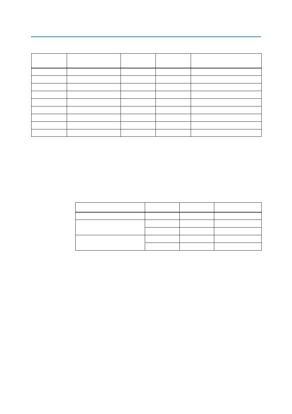
Table 2–33. Power Inputs
Power Source
Voltage (V)
Current (A)
Maximum Wattage (W)
Laptop-style DC input
15.0
4.3
65
25-W PCI Express edge connector
3.3
3.0
9
12.0
2.1
16
75-W PCI Express edge connector
3.3
3.0
9
12.0
5.5
66