2 configuration pins, 1 chip mode, 2 cpu_clk mode – BECKHOFF ET1200 User Manual
Page 23: 3 tx shift, Configuration pins, Chip mode, Cpu_clk mode, Tx shift, Table 11: chip mode, Table 12: cpu_clk mode
Pin Description
Slave Controller
– ET1200 Hardware Description
III-13
3.2
Configuration Pins
The configuration pins are used to configure the ET1200 at power-on with pull-up or pull down
resistors. At power-on the ET1200 uses these pins as inputs to latch the configuration
4
. After power-
on, the pins have their operation functionality which has been assigned to them, and therefore pin
direction changes if necessary. The power-on phase finishes before the nRESET pin is released. In
subsequent reset phases without power-on condition, the configuration pins still have their operation
functionality, i.e., the ET1200 configuration is not latched again and output drivers remain active.
The configuration value 0 is realized by a pull-down resistor, a pull-up resistor is used for a 1. Since
some configuration pins are also used as LED outputs, the polarity of the LED output depends on the
configuration value.
3.2.1
Chip mode
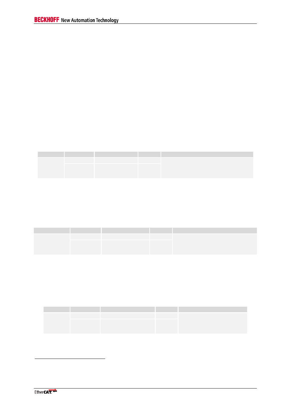
Chip mode configures the type of the two permanent ports 0 and 1. It is shown in Table 11. The Chip
mode affects the number of available PDI signals.
Chip mode is shown in Table 11.
Table 11: Chip Mode
Description
Config signal
Pin name
Register
MODE[1:0] Values
Chip Mode
MODE[0]
LINKACT(0)/MODE[0]
0x0E00[0]
00 = EBUS/EBUS (port 0 = EBUS, port 1 = EBUS)
01 = reserved
10 = MII/EBUS (port 0 = MII, port 1 = EBUS)
11 = EBUS/MII (port 0 = EBUS, port 1 = MII)
MODE[1]
LINKACT(1)/MODE[1]
0x0E00[1]
3.2.2
CPU_CLK MODE
CLK_MODE is used to provide a clock signal to an external microcontroller. If CLK_MODE is not 00,
CPU_CLK is available on PDI[7], thus this pin is not available for PDI signals anymore.
The CPU_CLK MODE is shown in Table 12.
Table 12: CPU_CLK Mode
Description
Config signal
Pin name
Register
Values
CPU_CLK MODE
CLK_MODE[0]
PERR(0)/CLK_MODE[0]
0x0E00[2]
00 = off, PDI[7]/CPU_CLK available for PDI
01 = 25 MHz clock output at PDI[7]/CPU_CLK
10 = 20 MHz clock output at PDI[7]/CPU_CLK
11 = 10 MHz clock output at PDI[7]/CPU_CLK
CLK_MODE[1
PERR(1)/CLK_MODE(1)
0x0E00[3]
3.2.3
TX Shift
Phase shift (0/10/20/30ns) of MII TX signals (TX_ENA, TX_D[3:0]) can be attained via the C25_SHI[x]
signals. TX Shift settings are explained in Table 13. It is recommended to support all C25_SHI[1:0]
configurations by hardware options to enable later adjustments.
Table 13: TX Shift
Description
Config signal
Pin name
Register
Values
TX Shift
C25_SHI[0]
PDI[10]/TX_D[2]/C25_SHI[0]
0x0E00[4]
00 = MII TX signals not delayed
01 = MII TX signals delayed by 10 ns
10 = MII TX signals delayed by 20 ns
11 = MII TX signals delayed by 30 ns
C25_SHI[1]
PDI[11]/TX_D[3]/C25_SHI[1]
0x0E00[5]
4
Take care of proper configuration: External devices attached to dual-purpose configuration pins might interfere
sampling the intended configuration if they are e.g. not properly powered at the sample time (external device
keeps configuration pin low although a pull-up resistor is attached). In such cases the ET1200 power-on value
sampling time can be delayed by delaying power activation.