Chip test five (ctest5), Register: 0x22 – Avago Technologies LSI53C1010R User Manual
Page 176
Advertising
4-58
Registers
Version 2.2
Copyright © 2000–2003 by LSI Logic Corporation. All rights reserved.
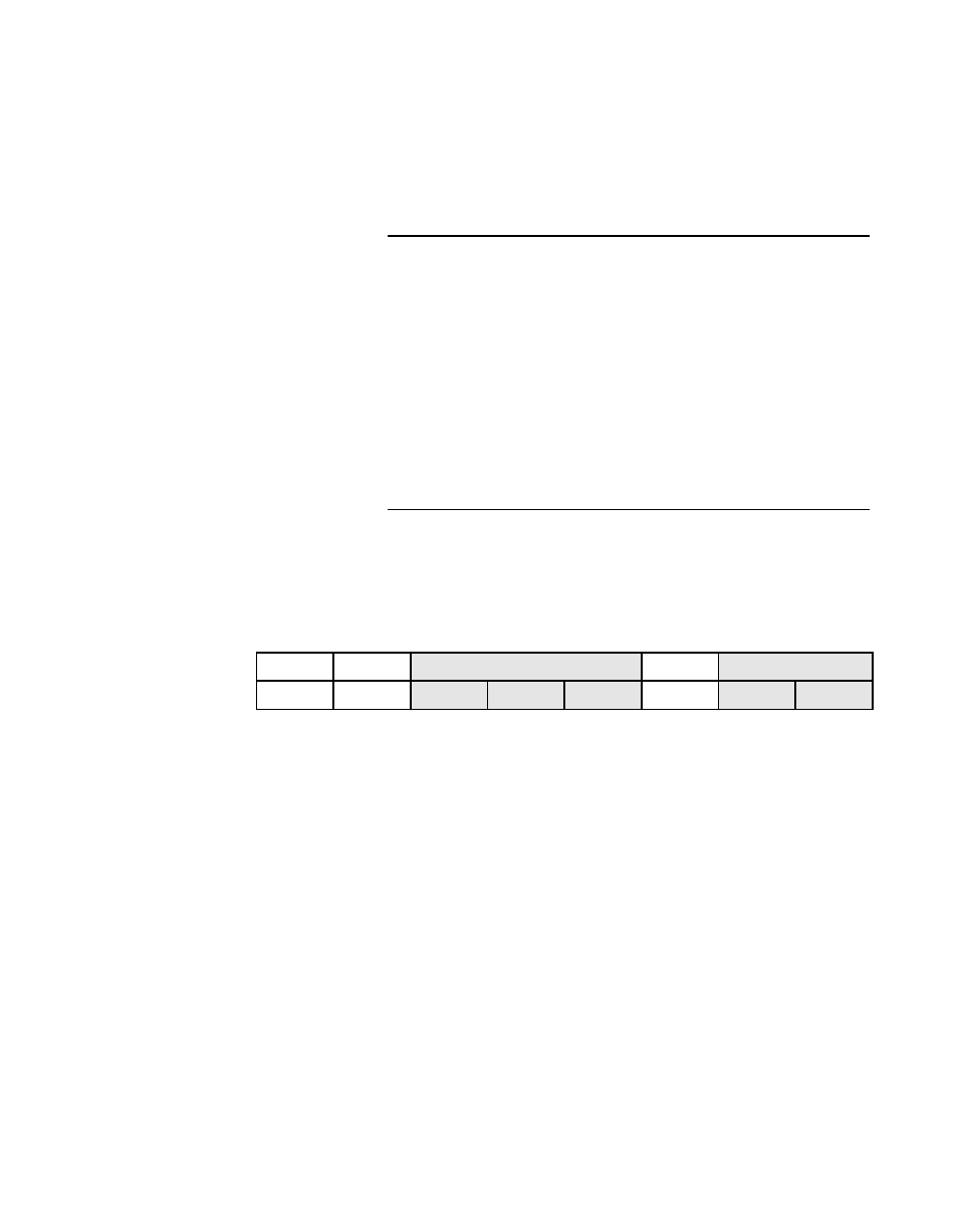
registers. Each of the eight bytes that make up the 64-bit
DMA FIFO is accessed by writing these bits to the proper
value. For normal operation, FBL3 must equal zero.
Register: 0x22
Chip Test Five (CTEST5)
Read/Write
ADCK
Clock Address Incrementor
7
Setting this bit increments the address pointer contained
in the
register. The DNAD
register is incremented based on the DNAD contents and
the current
value. This bit
automatically clears itself after incrementing the
DNAD register.
FBL3
FBL2
FBL1
FBL0
DMA FIFO
Byte Lane
Pins
0
x
x
x
Disabled
N/A
1
0
0
0
0
D[7:0]
1
0
0
1
1
D[15:8]
1
0
1
0
2
D[23:16]
1
0
1
1
3
D[31:24]
1
1
0
0
4
D[39:32]
1
1
0
1
5
D[47:40]
1
1
1
0
6
D[53:48]
1
1
1
1
7
D[63:54]
7
6
5
3
2
1
0
ADCK
BBCK
R
BL2
R
0
0
0
0
0
0
0
0
Advertising