Altera Internal Memory (RAM and ROM) IP Core User Manual
Page 13
Embedded Memory Blocks
Write Operation
(4)
Read Operation
MLAB
Falling clock edges
Rising clock edges (in Arria
V, Cyclone V, and Stratix V
devices only)
Rising clock edges
(5)
M-RAM
Rising clock edges
Rising clock edges
M4K
Falling clock edges
Rising clock edges
M512
Falling clock edges
Rising clock edges
It is important that you understand the write operation triggering to avoid potential write contentions
that can result in unknown data storage at that location.
These figures show the valid write operation that triggers at the rising and falling clock edge, respectively.
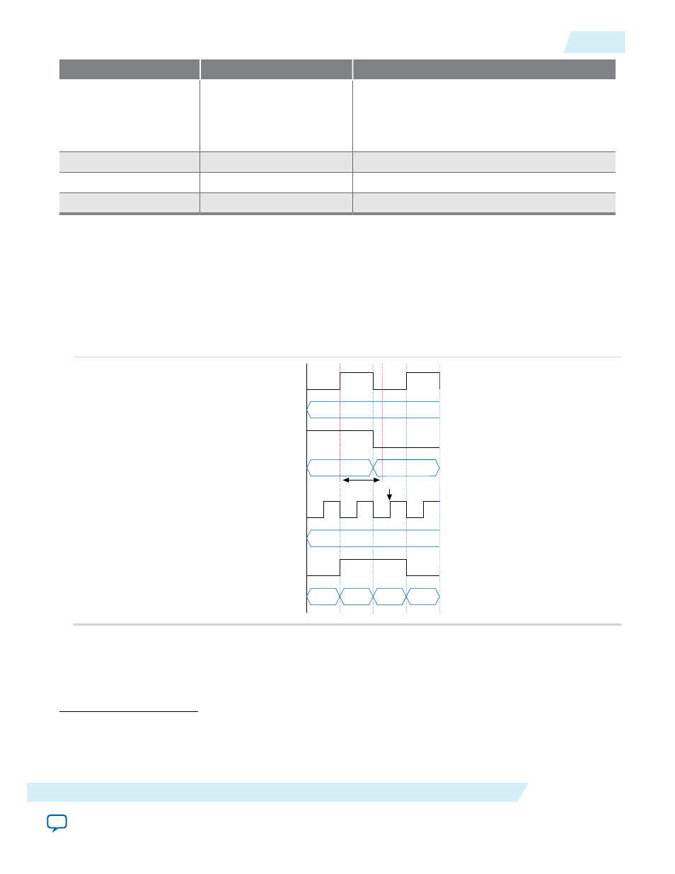
Figure 3-1: Valid Write Operation that Triggers at Rising Clock Edges
This figure assumes that t
wc
is the maximum write cycle time interval. Write operation of data 03 through
port B does not meet the criteria and causes write contention with the write operation at port A, which
result in unknown data at address 01. The write operation at the next rising edge is valid because it meets
the criteria and data 04 replaces the unknown data.
clock_a
address_a
wren_a
data_a
clock_b
address_b
wren_b
data_b
twc
Valid Write
01
05
06
01
02
03
04
05
(4)
Write operation triggering is not applicable to ROMs.
(5)
MLAB supports continuos reads. For example, when you write a data at the write clock rising edge and after
the write operation is complete, you see the written data at the output port without the need for a read clock
rising edge.
UG-01068
2014.12.17
Write and Read Operations Triggering
3-3
Embedded Memory Functional Description
Altera Corporation