Altera Internal Memory (RAM and ROM) IP Core User Manual
Page 55
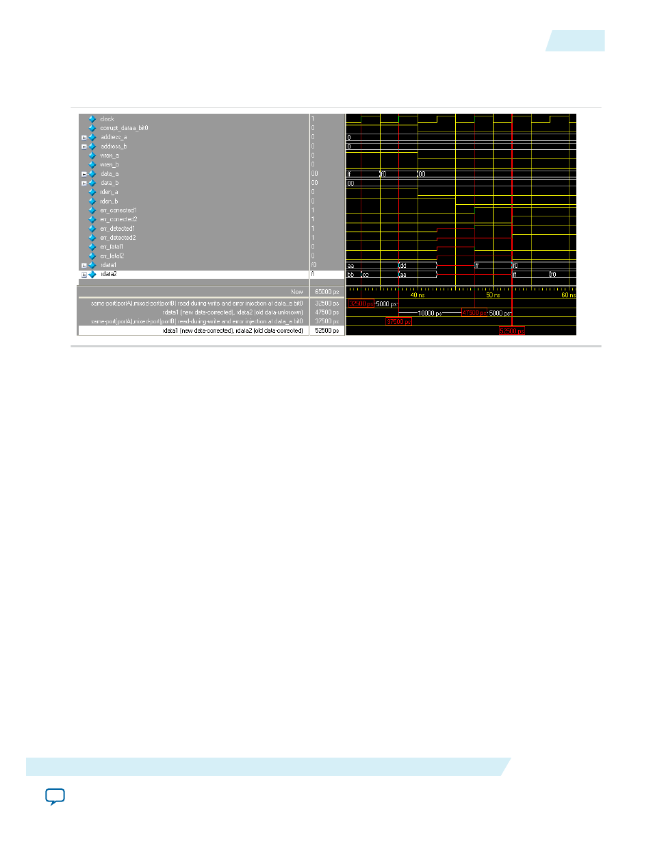
Figure 5-5: Error Injection– Asserting corrupt_dataa_bit0
This figure shows the timing diagram of the effect when an error is injected to twist the LSB of the
encoded data at port A by asserting
corrupt_dataa_bit0
.
At 32500 ps, same-port read-during-write occurs at port A while mixed-port read-during-write occurs at
port B. The
corrupt_dataa_bit0
is also asserted to corrupt the LSB of encoded data at port A; therefore,
the storing data has the LSB corrupted, in which the intended data
ff
is corrupted, becomes
fe
, and
stored at address 0. After four clock cycles at 47500 ps, the
rdata1
port shows the new data
ff
that has
been corrected by the decoder, and the ECC status signals,
err_corrected1
and
err_detected1
, are
asserted. For
rdata2
port, old data (which is unknown) is shown and the ECC-status signal remains
unknown.
Note: The decoders correct the single-bit error of the data shown at
rdata1
and
rdata2
ports only. The
actual data stored at address 0 in the RAM remains corrupted, until new data is written.
At 37500 ps, the same condition happens to port A and port B. The difference is port B reads the
corrupted old data
fe
from address 0. After four clock cycles at 52500 ps, the
rdata2
port shows the old
data ff that has been corrected by the decoder and the ECC status signals,
err_corrected2
and
err_detected2
, are asserted to show the data has been corrected.
UG-01068
2014.12.17
Simulation Results
5-9
Design Example
Altera Corporation