Byte enable, Byte enable -8 – Altera Internal Memory (RAM and ROM) IP Core User Manual
Page 18
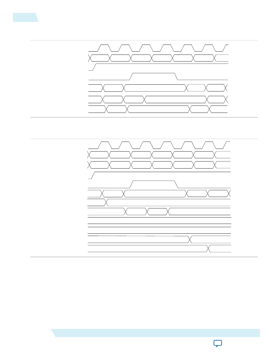
Figure 3-4: Address Clock Enable During Read Cycle Waveform
This figure shows the address clock enable waveform during the read cycle.
inclock
rden
rdaddress
q (synch)
a0
a1
a2
a3
a4
a5
a6
q (asynch)
an
a0
a4
a5
latched address
(inside memory)
dout0
dout1
dout4
dout4
dout5
addressstall
a1
doutn-1
doutn
doutn
dout0
dout1
Figure 3-5: Address Clock Enable During the Write Cycle Waveform
This figure shows the address clock enable waveform during the write cycle.
inclock
wren
wraddress
a0
a1
a2
a3
a4
a5
a6
an
a0
a4
a5
latched address
(inside memory)
addressstall
a1
data
00
01
02
03
04
05
06
contents at a0
contents at a1
contents at a2
contents at a3
contents at a4
contents at a5
XX
04
XX
00
03
01
XX
02
XX
XX
XX
05
Byte Enable
All embedded memory blocks that are implemented as RAMs support byte enables that mask the input
data so that only specific bytes, nibbles, or bits of data are written. The unwritten bytes or bits retain the
previously written value.
The LSB of the byte-enable port corresponds to the LSB of the data bus. For example, if you use a RAM
block in x18 mode and the byte-enable port is 01, data [8..0] is enabled and data [17..9] is disabled.
Similarly, if the byte-enable port is 11, both data bytes are enabled.
3-8
Byte Enable
UG-01068
2014.12.17
Altera Corporation
Embedded Memory Functional Description