Memory blocks address clock enable support, Memory blocks address clock enable support -7 – Altera Internal Memory (RAM and ROM) IP Core User Manual
Page 17
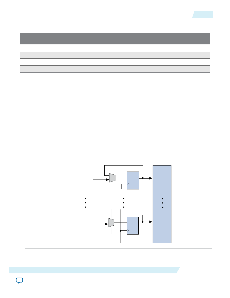
Table 3-5: Clocking Modes
This table lists the embedded memory clocking modes.
Clocking Modes
Single-port
RAM
Simple Dual-
port RAM
True Dual-port
RAM
Single-port
ROM
Dual-port ROM
Single clock
Supported
Supported
Supported
Supported
Supported
Read/Write
—
Supported
—
—
—
Input/Output
Supported
Supported
Supported
Supported
Supported
Independent
—
—
Supported
—
Supported
Note: Asynchronous clock mode is only supported in MAX series of devices, and not supported in Stratix
and newer devices. However, Stratix III and newer devices support asynchronous read memory for
simple dual-port RAM mode if you choose MLAB memory block with unregistered
rdaddress
port.
Note: The clock enable signals are not supported for write address, byte enable, and data input registers
on Arria V, Cyclone V, and Stratix V MLAB blocks.
Memory Blocks Address Clock Enable Support
The embedded memory blocks support address clock enable, which holds the previous address value for
as long as the signal is enabled (
addressstall = 1
). When the memory blocks are configured in dual-
port mode, each port has its own independent address clock enable. The default value for the address
clock enable signal is low (disabled).
Figure 3-3: Address Clock Enable
This figure shows an address clock enable block diagram. The address clock enable is referred to by the
port name
addressstall
.
address[0]
address[N]
addressstall
clock
1
0
address[0]
register
address[N]
register
address[N]
address[0]
1
0
UG-01068
2014.12.17
Memory Blocks Address Clock Enable Support
3-7
Embedded Memory Functional Description
Altera Corporation