Port width configurations, Port width configurations -4 – Altera Internal Memory (RAM and ROM) IP Core User Manual
Page 14
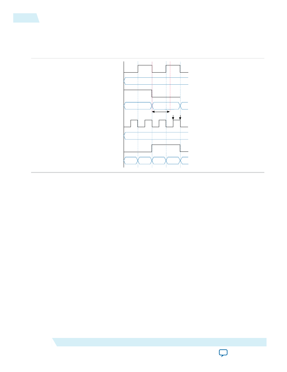
Figure 3-2: Valid Write Operation that Triggers at Falling Clock Edges
This figure assumes that t
wc
is the maximum write cycle time interval. Write operation of data 04 through
port B does not meet the criteria and therefore causes write contention with the write operation at port A
that result in unknown data at address 01. The next data (05) is latched at the next rising clock edge that
meets the criteria and is written into the memory block at the falling clock edge.
clock_a
address_a
wren_a
data_a
clock_b
address_b
wren_b
data_b
t
Actual Write
01
05
06
01
02
03
04
05
wc
Valid Write
Note: Data and addresses are latched at the rising edge of the write clock regardless of the different write
operation triggering.
Port Width Configurations
The following equation defines the port width configuration: Memory depth (number of words) × Width
of the data input bus.
• If your port width configuration (either the depth or the width) is more than the amount an internal
memory block can support, additional memory blocks (of the same type) are used. For example, if you
configure your M9K as 512 × 36, which exceeds the supported port width of 512 × 18, two M9Ks are
used to implement your RAM.
• In addition to the supported configuration provided, you can set the memory depth to a non-power of
two, but the actual memory depth allocated can vary. The variation depends on the type of resource
implemented.
• If the memory is implemented in dedicated memory blocks, setting a non-power of two for the
memory depth reflects the actual memory depth.
• When you implement your memory using dedicated memory blocks, refer to the Fitter report to check
the actual memory depth.
3-4
Port Width Configurations
UG-01068
2014.12.17
Altera Corporation
Embedded Memory Functional Description