Altera Internal Memory (RAM and ROM) IP Core User Manual
Page 22
RDW Operation
Description
Mixed-Port
RDW
The mixed-port RDW occurs when one port reads and another port writes to the same
address location with the same clock. The mixed-port RDW has the following output
choices:
• Old Data—The RAM outputs reflect the old data at that address before the write
operation proceeds. Old Data is supported for single clock configuration only.
• Don't Care—The RAM outputs “don't care” or “unknown” values for RDW
operation without analyzing the timing path.
For LUTRAM, this option functions differently whereby when you enable this option,
the RAM outputs “don’t care” or “unknown” values for RDW operation but analyzes
the timing path to prevent metastability. Therefore, if you want the RAM to output
“don’t care” values without analyzing the timing path, you have to turn on the Do not
analyze the timing between write and read operation. Metastability issues are
prevented by never writing and reading at the same address at the same time
option.
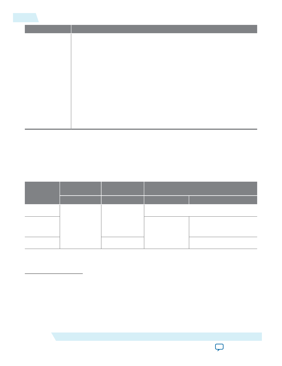
Selecting RDW Output Choices for Various Memory Blocks
The available output choices for the RDW behavior vary, depending on the types of RDW and embedded
memory block in use.
Table 3-9: Output Choices for the Same-Port and Mixed-Port Read-During-Write
This table lists ists the available output choices for the same-port, and mixed-port RDW for various embedded
memory blocks.
Memory Block
Types
Single-port RAM
(9)
Simple dual-port
RAM
(10)
True dual-port RAM
Same port RDW
Mixed-port RDW
Same port RDW
(11)
Mixed-port RDW
(12)
M512
No parameter
editor
(13)
Old Data
Don’t Care
N/A
M4K
No parameter
editor
(13)
Old Data
Don’t Care
M-RAM
Don’t Care
Don’t Care
(9)
Single-port RAM only supports same-port RDW, and the clocking mode must be either single clock mode,
or input/output clock mode.
(10)
Simple dual-port RAM only supports mixed-port RDW, and the clocking mode must be either single clock
mode, or input/output clock mode.
(11)
The clocking mode must be either single clock mode, input/output clock mode, or independent clock mode.
(12)
The clocking mode must be either single clock mode, or input/output clock mode.
(13)
There is no option page available from the parameter editor in this mode. By default, the new data flows
through to the output.
3-12
Selecting RDW Output Choices for Various Memory Blocks
UG-01068
2014.12.17
Altera Corporation
Embedded Memory Functional Description