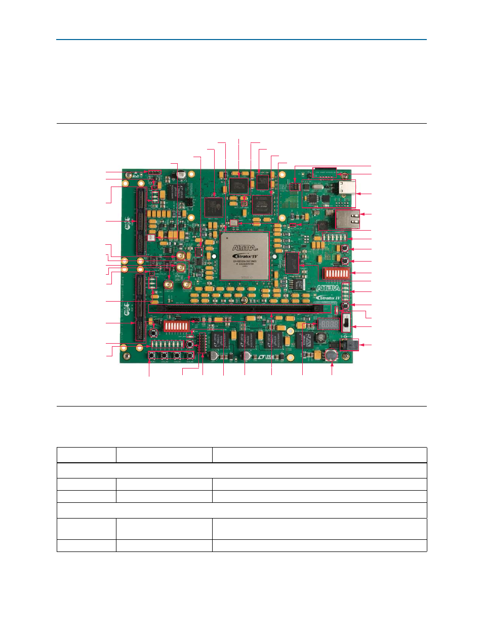
Board overview, Board overview –2, Figure 2–1 – Altera Stratix IV E FPGA Development Board User Manual
Page 10: Table 2–1
2–2
Chapter 2: Board Components
Board Overview
Stratix IV E FPGA Development Board Reference Manual
May 2011
Altera Corporation
Board Overview
This section provides an overview of the Stratix IV E FPGA development board,
including an annotated board image and component descriptions.
provides an overview of the development board features.
describes the components and lists their corresponding board references.
Figure 2–1. Overview of the Stratix IV E FPGA Development Board Features
HSMC Port A JTAG
Header (J15)
Character
LCD
Header
(J23)
System
Reset
Push-Button
Switch (S5)
Max II CPLD EPM2210 System Controller (U10)
DDR3 SDRAM
DIMM x72
Memory (J20)
Stratix IV E FPGA (U19)
HSMC Port B (J9)
Clock Input SMA (J17)
Speaker Header (J1)
HSMC Port A (J19)
HSMC Port B JTAG
Header (J5)
Fan Header (J12)
100 MHz Oscillator (X2)
QDRII+ x18 Memory (U11)
DC Input Jack (J22)
Power Switch (SW3)
Embedded USB-Blaster
Circuitry (J6)
JTAG Connector
(J24)
CLKIN_P SMA (J13)
HSMC Port B
Status LEDs
(D3, D4, D5)
CLKIN_N SMA (J14)
Clock Output SMA (J16)
HSMC Port A
Status LEDs
(D13, D14, D16)
CPU Reset Push-Button
Switch (S4)
User LEDs (D23-D30)
Gigabit Ethernet
Port (J8)
Ethernet LEDs
(D7-D12)
Reset Configuration
Push-Button Switch (S1)
MAX II DIP Switch (SW2)
MAX II LEDs
(D15, D17-D20)
User 1/User 2
Push-Button Switch (S3)
Power LED (D21)
Rotary Switch
(SW5)
Quad 7-Segment
Display
(U29)
User DIP
Switch
(SW4)
RLDRAM II CIO x36 (U24)
MAX II JTAG Header
(J10)
Factory Configuration
Push-Button Switch (S2)
User
Push-Button
Switches
(S6-S9)
66 MHz Oscillator (X3)
SSRAM x36 Memory (U3)
Flash x16 Memory (U2)
100 MHz Oscillator for MAX II (Y2)
Clock Enable DIP
Switch (SW1)
Configuration
Done
LED
(D22)
Table 2–1. Stratix IV E FPGA Development Board Components (Part 1 of 4)
Board Reference
Type
Description
Featured Devices
U19
FPGA
EP4SE530H35, 1152-pin FBGA.
U10
CPLD
EPM2210F256, 256-pin FBGA.
Configuration, Status, and Setup Elements
J6
USB type-B connector
USB interface for programming the FPGA through embedded
USB-Blaster JTAG via a type-B USB cable.
J24
JTAG connector (bottom side)
Disables embedded blaster (for use with external USB-Blasters).