Components and interfaces, 10/100/1000 ethernet, Components and interfaces –31 – Altera Stratix IV E FPGA Development Board User Manual
Page 39: 10/100/1000 ethernet –31
Chapter 2: Board Components
2–31
Components and Interfaces
May 2011
Altera Corporation
Stratix IV E FPGA Development Board Reference Manual
Components and Interfaces
This section describes the development board's communication ports and interface
cards relative to the Stratix IV E FPGA device. The development board supports the
following communication ports:
■
10/100/1000 Ethernet
■
Embedded USB-Blaster
■
HSMC
10/100/1000 Ethernet
The development board incorporates a triple speed 10/100/1000 BASE-T Ethernet
port. This implementation uses a discrete Ethernet PHY (Marvell 88E1111) device and
RJ45 connector with integrated magnetics connected to the FPGA. The Marvell
88E1111 PHY device is an auto-negotiating Ethernet PHY with a GMII, RGMII, or
SGMII interface to the FPGA. The MAC function must be provided in the FPGA for
typical networking applications. The device uses 2.5-V and 1.1-V power rails and
requires a 25-MHz reference clock driven from a dedicated oscillator.
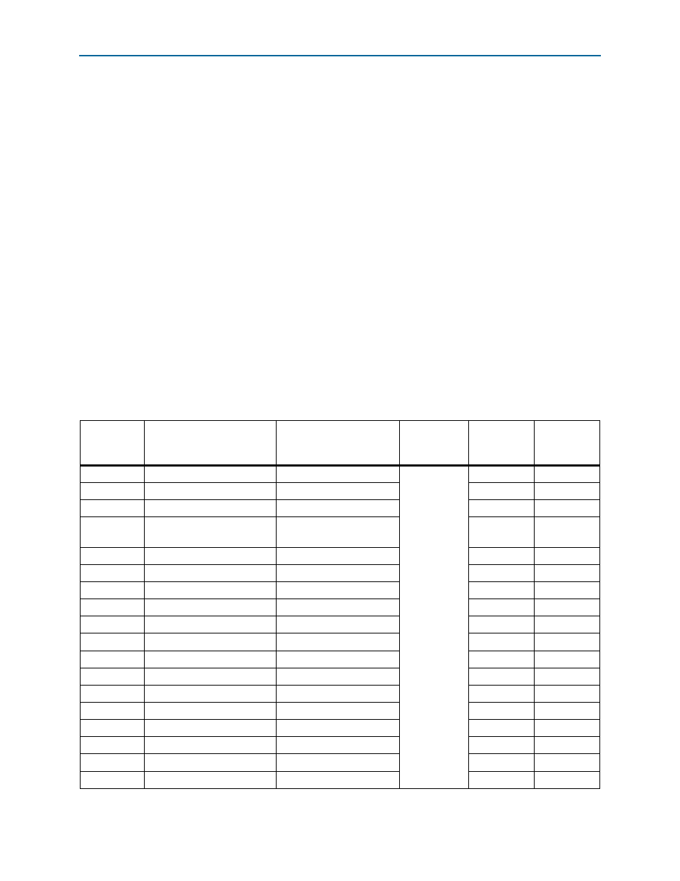
lists the SGMII and RGMII interface pin assignments to the FPGA for the
Ethernet PHY device.
Table 2–37. Ethernet PHY Pin Assignments, Signal Names and Functions
Board
Reference
Description
Schematic Signal Name
I/O Standard
Stratix IV E
Device
Pin Number
Other
Connections
U15.8
RGMII transmit clock
ENET_GTX_CLK
2.5-V
M33
—
U15.23
Management bus interrupt
ENET_INTn
F32
—
U15.70
Duplex/Collision LED
ENET_LED_DUPLEX
—
—
U15.76
10 Mb Link LED
ENET_LED_LINK10
—
U15.64,
U15.59
U15.74
100 Mb Link LED
ENET_LED_LINK100
—
—
U15.73
1000 Mb Link LED
ENET_LED_LINK1000
—
U15.69
RX Data Active LED
ENET_LED_RX
—
U15.65
U15.68
TX Data Active LED
ENET_LED_TX
—
U15.61
U15.25
Management bus data clock
ENET_MDC
K34
—
U15.24
Management bus data
ENET_MDIO
N27
—
U15.28
Device reset
ENET_RESETn
M31
—
U15.30
Reset
ENET_RSET
—
—
U15.2
RSGMII receive clock
ENET_RX_CLK
K32
—
U15.83
GMII collision
ENET_RX_COL
J31
—
U15.84
GMII carrier sense
ENET_RX_CRS
K33
—
U15.95
RSGMII receive data bus
ENET_RX_D0
M24
—
U15.92
RSGMII receive data bus
ENET_RX_D1
P34
—
U15.93
RSGMII receive data bus
ENET_RX_D2
J34
—