Development board block diagram, Handling the board – Altera Stratix IV E FPGA Development Board User Manual
Page 8
1–4
Chapter 1: Overview
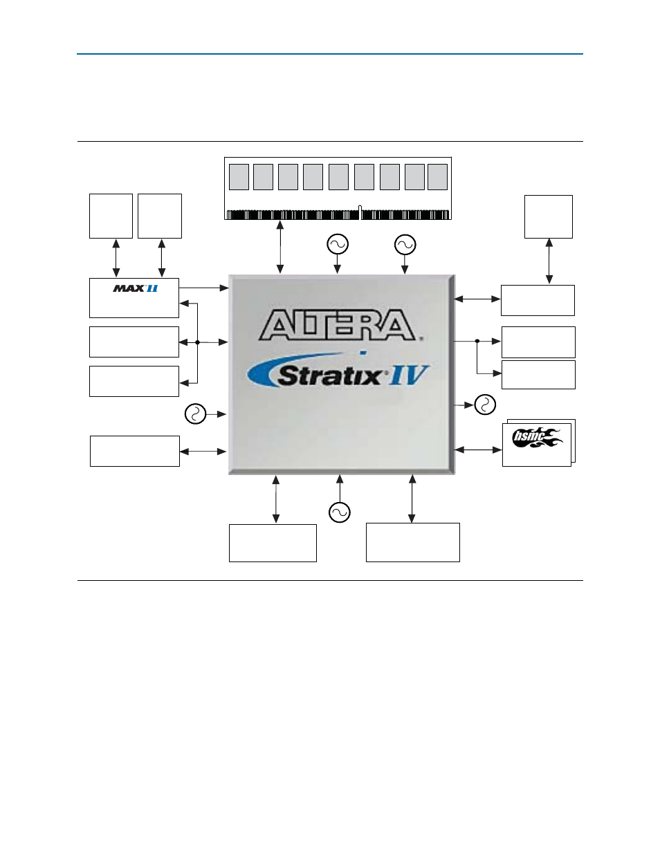
Development Board Block Diagram
Stratix IV E FPGA Development Board Reference Manual
May 2011
Altera Corporation
Development Board Block Diagram
shows the block diagram of the Stratix IV E FPGA development board.
Handling the Board
When handling the board, it is important to observe the following static discharge
precaution:
c
Without proper anti-static handling, the board can be damaged. Therefore, use
anti-static handling precautions when touching the board. The Stratix IV E FPGA
development board must be stored in a temperature of between –40° C and 100° C.
The recommended operating temperature is between 0° C and 55° C.
Figure 1–1. Stratix IV E FPGA Development Board Block Diagram
EP4SE530H35
10/100/1000
Ethernet
128 x 64
Graphic Display
RLDRAM II CIO
(x36)
Quad 7-Seg,
User LEDs Push-Button
Switches
14-pin LCD
Header
CPLD
(x32)
64 MB Flash
(x16)
4 MB SSRAM
(x32)
RJ45
Jack
Power
Measure
2.5 V
CMOS
2.5 V
CMOS
CMOS +
LVDS
2.5 V
CMOS
1.5 V/1.8 V
HSTL
2.5 V CMOS
1.5 V
SSTL
CMOS +
LVDS
100 MHz
XTAL
Port
USB
Blaster
66 MHz XTAL
4 MB QDR II+
(x18)
SMA Input
1.5 V/1.8 V
HSTL
125 MHz XTAL
SMA Output
2 GB DDR3 SDRAM DIMM (x72)