Rldram ii cio, Rldram ii cio –49 – Altera Stratix IV E FPGA Development Board User Manual
Page 57
Chapter 2: Board Components
2–49
Memory
May 2011
Altera Corporation
Stratix IV E FPGA Development Board Reference Manual
lists the QDR II+ SRAM component reference and manufacturing
information.
RLDRAM II CIO
The RLDRAM II CIO is a 576-Mb RLDRAM II memory interface with a 36-bit data bus
width. This memory interface is designed to run at a maximum frequency of
400 MHz. The default I/O voltage for the RLDRAM II CIO device and the Stratix IV E
FPGA is 1.5 V. Placing a shunt on jumper J11 provides 1.8 V for VDDQ.
U11.E3
Read data bit
QDRII_Q11
1.5-V HSTL Class I
G8
U11.F2
Read data bit
QDRII_Q12
G11
U11.G3
Read data bit
QDRII_Q13
B2
U11.K3
Read data bit
QDRII_Q14
B5
U11.L2
Read data bit
QDRII_Q15
F6
U11.N3
Read data bit
QDRII_Q16
C5
U11.P3
Read data bit
QDRII_Q17
D6
U11.P6
Read data valid
QDRII_QVLD
A2
U11.A8
Read port select
QDRII_RPSn
K16
U11.A4
Write port select
QDRII_WPSn
D17
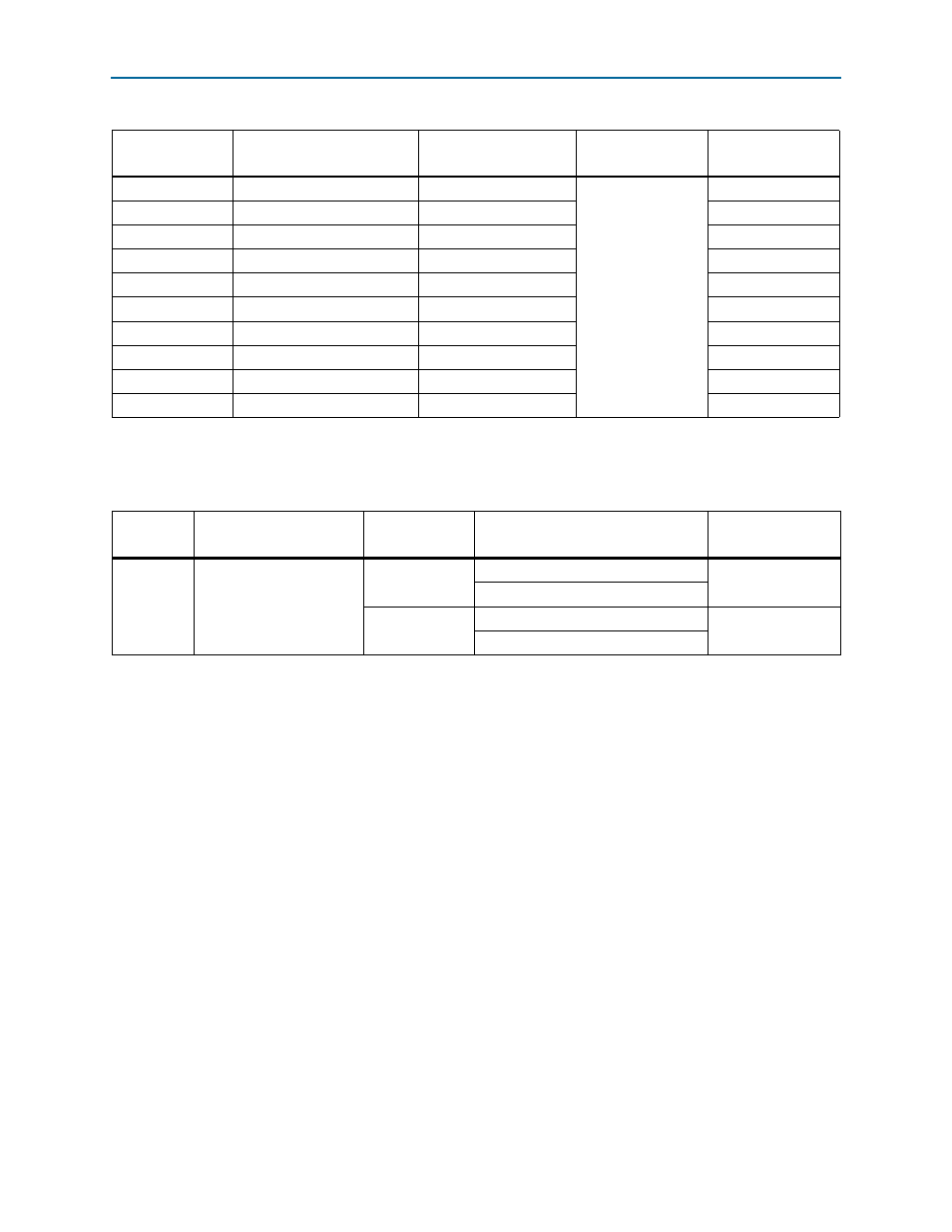
Table 2–45. QDR II+ SRAM Pin Assignments, Schematic Signal Names, and Functions (Part 3 of 3)
Board Reference
Description
Schematic Signal Name
I/O Standard
Stratix IV E Device
Pin Number
Table 2–46. QDR II+ SRAM Component Reference and Manufacturing Information
Board
Reference
Description
Manufacturer
Manufacturing
Part Number
Manufacturer
Website
U11
QDR II+ 4M x18, 400 MHz,
BGA-165
Cypress
Semiconductor
CY7C15632V18-400BZXC
CY7C15632V18-450BZXC
NEC
UPD44647186AF5-E25-FQ1-SSA
UPD44647186AF5-E22-FQ1-SSA