Memory, Ddr3, Memory –42 – Altera Stratix IV E FPGA Development Board User Manual
Page 50: Ddr3 –42
2–42
Chapter 2: Board Components
Memory
Stratix IV E FPGA Development Board Reference Manual
May 2011
Altera Corporation
lists the HSMC connector component reference and manufacturing
information.
Memory
This section describes the board's memory interface support, signal names, types, and
connectivity relative to the Stratix IV E FPGA device. The board has the following
memory interfaces:
■
DDR3
■
QDR II+
■
RLDRAM II CIO
■
SSRAM
■
Flash
f
For more information about the memory interfaces, refer
.
DDR3
There is a single DDR3 SDRAM DIMM on the board, providing a dual rank 2-GB
interface with a 72-bit data bus width on the vertical I/O banks. This memory
interface is designed to run at a maximum frequency of 533 MHz.
lists the DDR3 pin assignments, signal names, and functions.
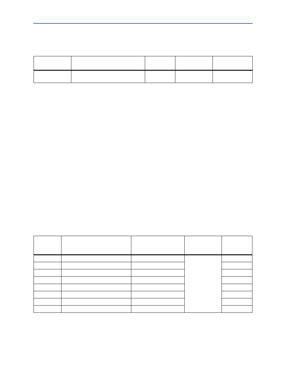
Table 2–42. HSMC Connector Component Reference and Manufacturing Information
Board Reference
Description
Manufacturer
Manufacturing
Part Number
Manufacturer
Website
J9 and J19
HSMC, custom version of QSH-DP
family high-speed socket.
Samtec
ASP-122953-01
Table 2–43. DDR3 Pin Assignments, Schematic Signal Names, and Functions (Part 1 of 5)
Board
Reference
Description
Schematic Signal Name
I/O Standard
Stratix IV E
Device
Pin Number
J20.188
Address bus
DDR3_DIMM_A0
1.5-V SSTL Class I
AL17
J20.181
Address bus
DDR3_DIMM_A1
AM17
J20.61
Address bus
DDR3_DIMM_A2
AL18
J20.180
Address bus
DDR3_DIMM_A3
AM18
J20.59
Address bus
DDR3_DIMM_A4
AN18
J20.58
Address bus
DDR3_DIMM_A5
AP18
J20.178
Address bus
DDR3_DIMM_A6
AL19
J20.56
Address bus
DDR3_DIMM_A7
AM19