Altera Stratix IV E FPGA Development Board User Manual
Page 42
2–34
Chapter 2: Board Components
Components and Interfaces
Stratix IV E FPGA Development Board Reference Manual
May 2011
Altera Corporation
The HSMC connector has a total of 172 pins, including 120 signal pins, 39 power pins,
and 13 ground pins. The ground pins are located between the two rows of signal and
power pins, acting both as a shield and a reference. The HSMC host connector is
based on the 0.5 mm-pitch QSH/QTH family of high-speed, board-to-board
connectors from Samtec. There are three banks in this connector. Bank 1 has every
third pin removed as done in the QSH-DP/QTH-DP series. Bank 2 and bank 3 have
all the pins populated as done in the QSH/QTH series.
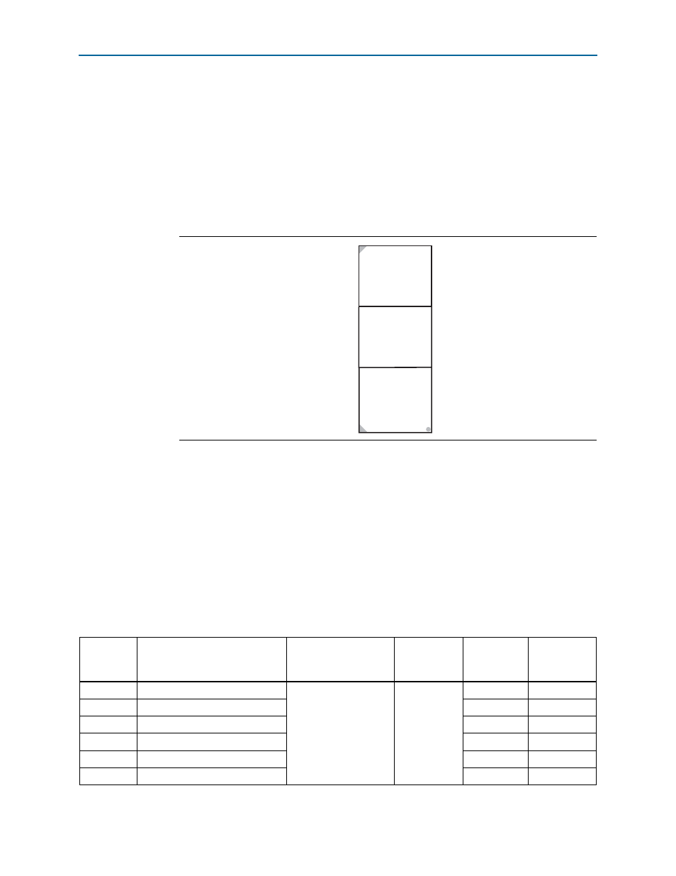
shows the bank arrangement of signals with respect to the Samtec
connector's three banks.
The HSMC interface has programmable bi-directional I/O pins that can be used as
2.5-V LVCMOS, which is 3.3-V LVTTL-compatible. These pins can also be used as
various differential I/O standards including, but not limited to, LVDS, mini-LVDS,
and RSDS with up to 17 full-duplex channels.
1
As noted in the
manual, LVDS and
single-ended I/O standards are only guaranteed to function when mixed according to
either the generic single-ended pin-out or generic differential pin-out.
lists the HSMC port A interface pin assignments, signal names, and
functions.
Figure 2–8. HSMC Signal and Bank Diagram
Bank 3
Power
D(79.40)
-or-
LVDS
CLKIN2, CLKOUT2
Bank 2
Power
D(39:0)
-or-
D[3:0] + LVDS
CLKIN1, CLKOUT1
Bank 1
8 TX Channels CDR
8 RX Channels CDR
JTAG
SMB
CLKIN0, CLKOUT0
Table 2–40. HSMC Port A Pin Assignments, Schematic Signal Names, and Functions (Part 1 of 5)
Board
Reference
Description
Schematic Signal
Name
I/O Standard
Stratix IV E
Device
Pin Number
Other
Connections
J19.1
Transceiver TX bit 7
NC
1.4-V PCML
—
—
J19.2
Transceiver RX bit 7
—
—
J19.3
Transceiver TX bit 7n
—
—
J19.4
Transceiver RX bit 7n
—
—
J19.5
Transceiver TX bit 6
—
—
J19.6
Transceiver RX bit 6
—
—