Ssram, Ssram –52 – Altera Stratix IV E FPGA Development Board User Manual
Page 60
2–52
Chapter 2: Board Components
Memory
Stratix IV E FPGA Development Board Reference Manual
May 2011
Altera Corporation
lists the RLDRAM II CIO component reference and manufacturing
information.
SSRAM
The SSRAM device consists of a single standard synchronous SRAM, providing 2-MB
memory interface with a 36-bit data bus. This device is part of the shared FSM bus
which connects to the flash memory, SSRAM, and MAX
II CPLD EPM2210 System
Controller. The device speed is 250-MHz single-data-rate.
U24.D10
Output data clock N
RLDC_QK_N0
Differential 1.5-V
HSTL Class I
AB32
U24.R3
Output data clock N
RLDC_QK_N1
AJ32
U24.D11
Output data clock P
RLDC_QK_P0
AB31
U24.R2
Output data clock P
RLDC_QK_P1
AJ31
U24.F12
Data valid
RLDC_QVLD
1.5-V HSTL Class I
AC32
U24.L1
Input reference voltage
RLDC_REFn
AD31
U24.M1
Write enable
RLDC_WEn
AE32
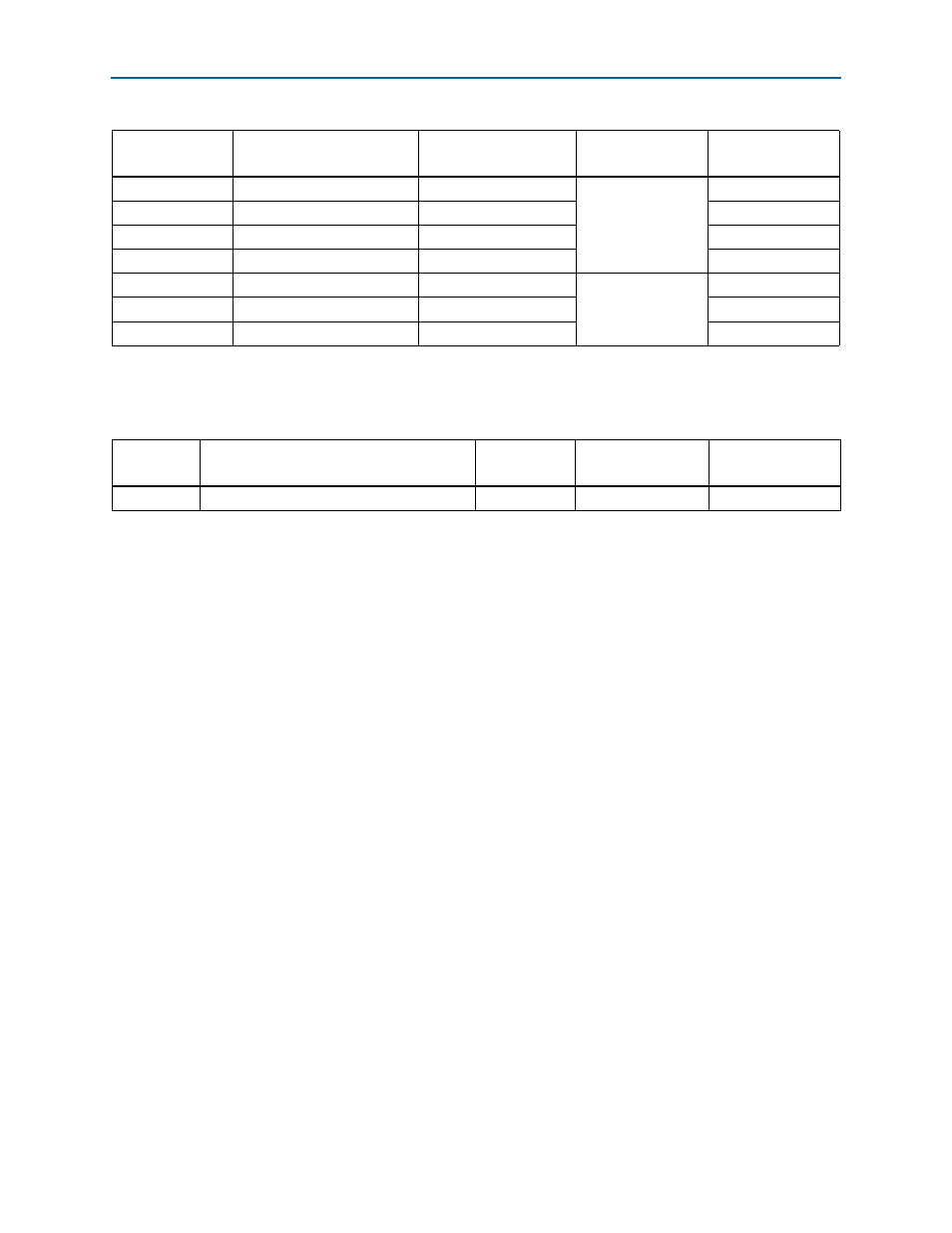
Table 2–47. RLDRAM II CIO Pin Assignments, Schematic Signal Names, and Functions (Part 3 of 3)
Board Reference
Description
Schematic Signal Name
I/O Standard
Stratix IV E Device
Pin Number
Table 2–48. RLDRAM II CIO Component Reference and Manufacturing Information
Board
Reference
Description
Manufacturer
Manufacturing
Part Number
Manufacturer
Website
U24
533 MHz RLDRAM II CIO 16M x36, BGA-144 Micron
MT49H16M36HT-18