Altera Stratix IV E FPGA Development Board User Manual
Page 12
2–4
Chapter 2: Board Components
Board Overview
Stratix IV E FPGA Development Board Reference Manual
May 2011
Altera Corporation
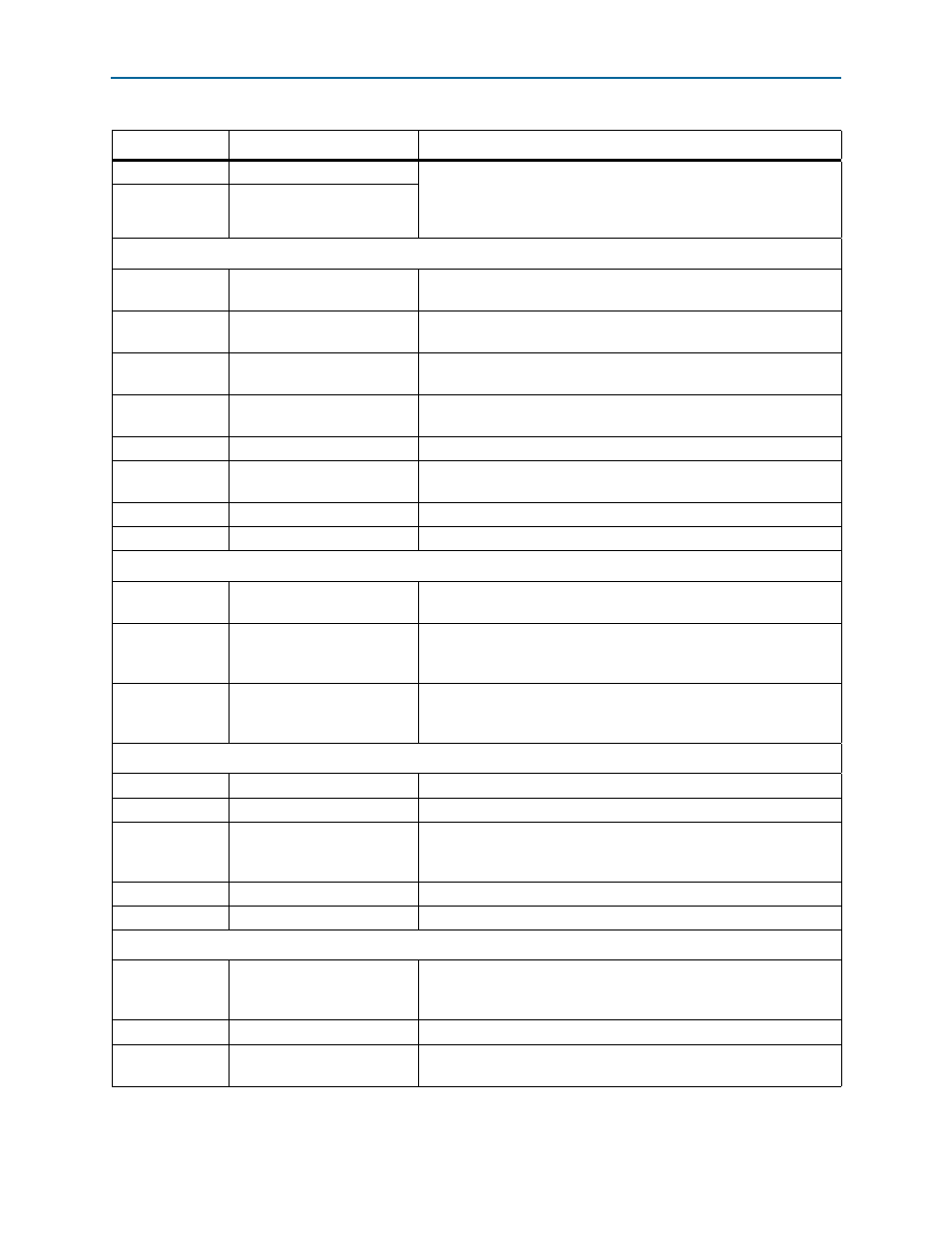
J13
CLKIN_P SMA (positive)
Drives LVPECL-compatible differential clock inputs into the LVDS clock
buffer (U22).The CLK66_SEL signal needs to be set to '1' on SW2 to
enable the SMA clock source. Two LVDS clocks are output from the
clock buffer to the FPGA.
J14
CLKIN_N SMA (negative)
General User Input/Output
SW4
User DIP switch
Connects directly to the FPGA. When the switch is ON, a logic 0 is
selected.
S1
Reset configuration
push-button switch
Press to reconfigure the FPGA from flash memory.
S2
Factory configuration
push-button switch
Press to reconfigure the FPGA to the factory default design.
S3
User 1 /User 2 push-button
switch
User-defined push-button switch. Driven to the MAX II CPLD EPM2210
System Controller.
S4
CPU reset push-button switch
Press to reset the FPGA logic.
S5
System reset push-button
switch
Press to reset the MAX II CPLD EPM2210 System Controller and FPGA
logic.
S6-S9
User push-button switches
Four user push-button switches. Driven low when pressed.
D23-D30
User LEDs
Illuminates when driven low.
Display Ports
J23
Character LCD header
Header which interfaces to the provided 16 character × 2 line LCD
module along with two standoffs.
U29
Seven-segment LED
Quad digit seven-segment LED display. The display is controlled by the
Stratix IV E FPGA device. Each segment of the display can be
illuminated by driving a logic 0 to the connected device's I/O pin.
J27
Graphics LCD connector
(bottom side)
Connector to plug in the flex cable from the 128 × 64 graphics display.
Lift the connector latch to plug in the flex cable, and then close the
latch.
Components and Interfaces
J19
HSMC port A
Provides 17 LVDS channels per the HSMC specification.
J9
HSMC port B
Provides 17 LVDS channels per the HSMC specification.
J8
Gigabit Ethernet
RJ-45 connector providing a 10/100/1000 Ethernet connection via a
Marvell 88E1111 PHY and interfaces to the FPGA-based Altera Triple
Speed Ethernet MegaCore function in SGMII mode.
J12
Fan header
Header to plug in the fan.
J1
Speaker header
Optional speaker header for user design.
Memory Devices
J20
DDR3 SDRAM DIMM x72
memory
DDR3 SDRAM DIMM (256 M x 72) 240-pin connector, populated with
a dual rank 2-GB memory module, and interfaces with a 72-bit data
width on the Vertical I/O (VIO) banks.
U24
RLDRAM II CIO x36 memory
533-MHz RLDRAM II CIO device in a 16 M x 36 configuration.
U11
QDR II+ x18 memory
QDR II+ SRAM device in a 4 M x 18 configuration for high-speed,
low-latency memory access.
Table 2–1. Stratix IV E FPGA Development Board Components (Part 3 of 4)
Board Reference
Type
Description