User dip switch, Clock enable dip switch, User dip switch –19 clock enable dip switch –19 – Altera Stratix IV E FPGA Development Board User Manual
Page 27
Chapter 2: Board Components
2–19
Configuration, Status, and Setup Elements
May 2011
Altera Corporation
Stratix IV E FPGA Development Board Reference Manual
User DIP Switch
Board reference SW4 is a 8-pin DIP switch. The switches in SW4 are user-defined and
provided for additional FPGA input control. There is no board-specific function for
these switches.
shows the user DIP switch controls and descriptions.
lists the user DIP switch component reference and manufacturing
information.
Clock Enable DIP Switch
The clock enable DIP switch (SW1) enables or disables the on-board oscillators.
shows the switch controls and descriptions.
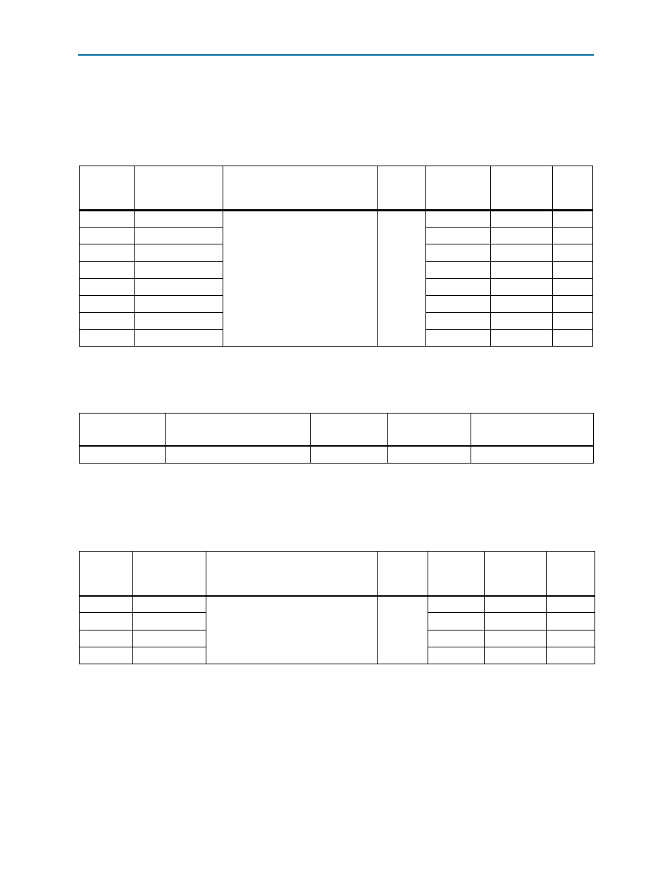
Table 2–12. User DIP Switch Controls
Board
Reference
Schematic Signal
Name
Description
I/O
Standard
Stratix IV E
Device Pin
Number
Other
Connections
Default
SW4.1
USER_DIPSW0
User-Defined DIP switch connected
to the FPGA device. When the
switch is in the OFF position, a
logic 1 is selected. When the
switch is in the ON position, a logic
0 is selected.
2.5-V
A28
—
ON
SW4.2
USER_DIPSW1
A19
—
ON
SW4.3
USER_DIPSW2
C18
—
ON
SW4.4
USER_DIPSW3
A20
—
ON
SW4.5
USER_DIPSW4
K19
—
ON
SW4.6
USER_DIPSW5
J19
—
ON
SW4.7
USER_DIPSW6
L19
—
ON
SW4.8
USER_DIPSW7
L20
—
ON
Table 2–13. User DIP Switch Component Reference and Manufacturing Information
Board Reference
Description
Manufacturer
Manufacturer
Part Number
Manufacturer Website
SW4
Eight-Position slide DIP switch
Grayhill
76SB08ST
Table 2–14. Clock Enable DIP Switch Controls
Board
Reference
Schematic
Signal Name
Description
I/O
Standard
Stratix IV E
Device Pin
Number
Other
Connections
Default
1
CLK50_EN
Clock enable DIP switch. When the
switch is in the OPEN or ENABLE
position, a logic 1 is selected. When the
switch is in the CLOSED or DISABLE
position, a logic 0 is selected.
2.5-V
—
U10.H3
ENABLE
2
CLK66_EN
—
U10.H4
ENABLE
3
CLK100_EN
—
U10.J1
ENABLE
4
CLK125_EN
—
U10.J2
ENABLE