Featured device: stratix iv e device, Featured device: stratix iv e device –5 – Altera Stratix IV E FPGA Development Board User Manual
Page 13
Chapter 2: Board Components
2–5
Featured Device: Stratix IV E Device
May 2011
Altera Corporation
Stratix IV E FPGA Development Board Reference Manual
Featured Device: Stratix IV E Device
The Stratix IV E FPGA development board features the Stratix IV E EP4SE530H35
device (U19) in a 1152-pin FBGA package.
f
For more information about the Stratix IV device family, refer to the
Table 2–2
describes the features of the Stratix IV E EP4SE530H35 device.
lists the Stratix IV E EP4SE530H35 component reference and manufacturing
information.
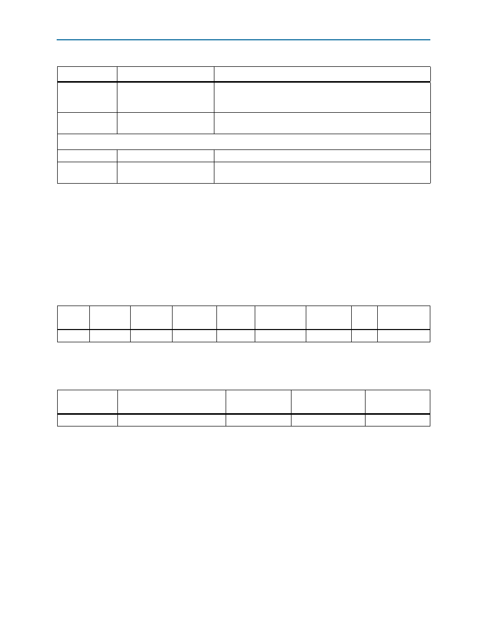
U3
SSRAM x36 memory
A single 250-MHz 18-Mb (2 M x 36) SSRAM device with a 165-BGA
package footprint. This footprint allows for both Flow-Through and
Pipelined devices (single or dual cycle deselect).
U2
Flash x16 memory
Embedded memory device which provides a 16-bit 64-MB non-volatile
memory port.
Power Supply
J22
DC input jack
Accepts a 14-V – 20-V DC power supply.
SW3
Power switch
Switch to power on or off the board when power is supplied from the
DC input jack.
Table 2–1. Stratix IV E FPGA Development Board Components (Part 4 of 4)
Board Reference
Type
Description
Table 2–2. Stratix IV E EP4SE530H35 Device Features
ALMs
Equivalent
LEs
M9K RAM
Blocks
M144K RAM
Blocks
Total RAM
bits
18-bit × 18-bit
Multipliers
Maximum
User I/O Pins
PLLs
Package Type
212,480
531,200
1,280
64
27,376
1,024
736
8
1152-pin FBGA
Table 2–3. Stratix IV E EP4SE530H35 Device Component Reference and Manufacturing Information
Board Reference
Description
Manufacturer
Manufacturing
Part Number
Manufacturer
Website
U19
FPGA, Stratix IV E F1152, leadfree
Altera
Corporation
EP4SE530H35C2N