Flash memory programming, Fpga programming from flash memory – Altera Stratix IV E FPGA Development Board User Manual
Page 22
2–14
Chapter 2: Board Components
Configuration, Status, and Setup Elements
Stratix IV E FPGA Development Board Reference Manual
May 2011
Altera Corporation
Flash Memory Programming
Flash memory programming is possible through a variety of methods using the
Stratix IV E device.
The default method is to use the factory design called the Board Update Portal. This
design is an embedded webserver, which serves the Board Update Portal web page.
The web page allows you to select new FPGA designs including hardware, software,
or both in an industry-standard S-Record File (.flash) and write the design to the user
hardware page (page 1) of the flash memory over the network.
The secondary method is to use the pre-built parallel flash loader (PFL) design
included in the development kit. The development board implements the Altera PFL
megafunction for flash memory programming. The PFL megafunction is a block of
logic that is programmed into an Altera programmable logic device (FPGA or CPLD).
The PFL functions as a utility for writing to a compatible flash memory device. This
pre-built design contains the PFL megafunction that allows you to write either page 0,
page 1, or other areas of flash memory over the USB interface using the Quartus II
software. This method is used to restore the development board to its factory default
settings.
Other methods to program the flash memory can be used as well, including the
Nios
®
II processor.
f
For more information on the Nios II processor, refe
of
the Altera website.
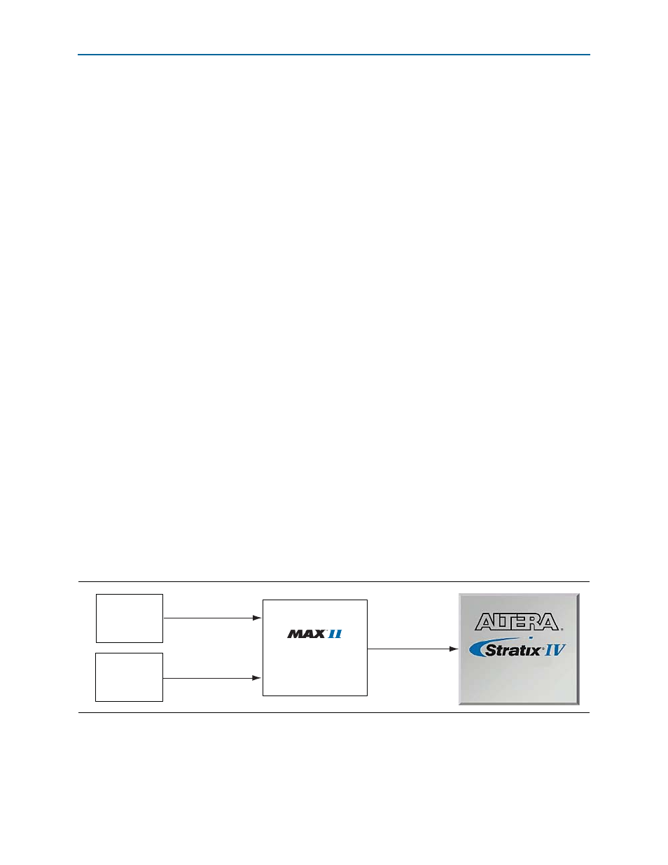
FPGA Programming from Flash Memory
On either power-up or by pressing the reset configuration push-button switch (S1),
the MAX
II CPLD EPM2210 System Controller's PFL configures the FPGA from the
flash memory. The PFL megafunction reads 16-bit data from the flash memory and
converts it to fast passive parallel (FPP) format. This 8-bit data is then written to the
FPGA's dedicated configuration pins during configuration. The bit stream loaded into
the FPGA is selected by the PGM rotary switch (SW5) connected to the MAX
II CPLD
EPM2210 System Controller.
illustrates the connection for FPGA programming from flash memory.
Figure 2–5. FPGA Programming from Flash Memory
EP4SE530H35
EPM2210F256
CPLD
Flash Memory
Rotary Switch
Flash Data
PGM
Fast Passive Parallel
(FPP)