Altera Stratix IV E FPGA Development Board User Manual
Page 58
2–50
Chapter 2: Board Components
Memory
Stratix IV E FPGA Development Board Reference Manual
May 2011
Altera Corporation
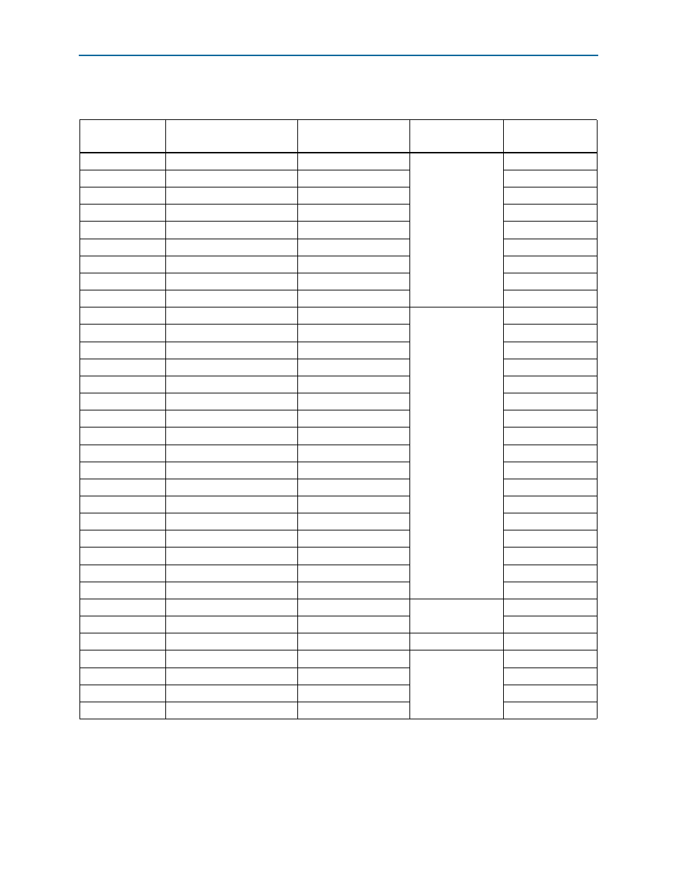
lists the RLDRAM II CIO pin assignments, signal names, and functions.
Table 2–47. RLDRAM II CIO Pin Assignments, Schematic Signal Names, and Functions (Part 1 of 3)
Board Reference
Description
Schematic Signal Name
I/O Standard
Stratix IV E Device
Pin Number
U24.G12
Address bus
RLDC_A0
1.5-V HSTL Class I
V25
U24.G11
Address bus
RLDC_A1
V24
U24.G10
Address bus
RLDC_A2
AB25
U24.H12
Address bus
RLDC_A3
AB24
U24.H11
Address bus
RLDC_A4
W26
U24.F1
Address bus
RLDC_A5
AB26
U24.G2
Address bus
RLDC_A6
AA33
U24.G3
Address bus
RLDC_A7
AA25
U24.G1
Address bus
RLDC_A8
AA34
U24.H2
Address bus
RLDC_A9
1.5-V HSTL Class I
AB27
U24.M12
Address bus
RLDC_A10
AH30
U24.M11
Address bus
RLDC_A11
AG30
U24.M10
Address bus
RLDC_A12
AH34
U24.L12
Address bus
RLDC_A13
AG33
U24.L11
Address bus
RLDC_A14
AH33
U24.P1
Address bus
RLDC_A15
AG34
U24.M2
Address bus
RLDC_A16
AD30
U24.M3
Address bus
RLDC_A17
AE31
U24.N1
Address bus
RLDC_A18
AF34
U24.N12
Address bus
RLDC_A19
AG29
U24.E12
Address bus
RLDC_A20
AA24
U24.E1
Address bus
RLDC_A21
W30
U24.D1
Address bus
RLDC_A22
W27
U24.J11
Bank address
RLDC_BA0
AC31
U24.K11
Bank address
RLDC_BA1
AC28
U24.H1
Bank address
RLDC_BA2
AB33
U24.K12
Input clock N
RLDC_CK_N
Differential 1.5-V
HSTL Class I
AF32
U24.J12
Input clock P
RLDC_CK_P
AF31
U24.L2
Chip select
RLDC_CSn
1.5-V HSTL Class I
AC29
U24.J2
Input data clock
RLDC_DK_N0
Differential 1.5-V
HSTL Class I
AB34
U24.K2
Input data clock
RLDC_DK_N1
AK34
U24.J1
Input data clock
RLDC_DK_P0
AC34
U24.K1
Input data clock
RLDC_DK_P1
AK33