Altera Stratix IV E FPGA Development Board User Manual
Page 16
2–8
Chapter 2: Board Components
MAX II CPLD EPM2210 System Controller
Stratix IV E FPGA Development Board Reference Manual
May 2011
Altera Corporation
3.3V_PG
2.5-V
E8
—
U9.G12
3.3-V power good monitor
CLK100_EN
2.5-V
J1
—
SW1.3, X2.1
100 MHz oscillator enable
CLK125_EN
2.5-V
J2
—
SW1.4, X4.1
125 MHz oscillator enable
CLK50_EN
2.5-V
H3
—
SW1.1, X5.1
50 MHz oscillator enable
CLK66_EN
2.5-V
H4
—
SW1.2, X3.1
66 MHz oscillator enable
CLK66_SEL
2.5-V
L14
—
SW2.8, U22.3
DIP-clock select SMA or oscillator
CLKIN_50
2.5-V
J12
J12
X5.3
50 MHz clock input
CLKIN_MAX_100
2.5-V
H12
—
Y2.3
100 MHz oscillator to the MAX II
CPLD EPM2210 System Controller
FACTORY_CONFIGn
2.5-V
A10
—
S2.2
Load factory or user design at
power-up
FLASH_ADVn
2.5-V
L13
D20
U2.F6
FSM bus flash memory address
valid
FLASH_CEn
2.5-V
K14
K25
U2.B4
FSM bus flash memory chip enable
FLASH_CLK
2.5-V
L15
K24
U2.E6
FSM bus flash memory clock
FLASH_OEn
2.5-V
M16
K23
U2.F8
FSM bus flash memory output
enable
FLASH_RDYBSYn
2.5-V
L11
C20
U2.F7
FSM bus flash memory ready
FLASH_RESETn
2.5-V
M15
G21
U2.D4
FSM bus flash memory reset
FLASH_WEn
2.5-V
L12
L22
U2.G8
FSM bus flash memory write enable
FPGA_CONF_DONE
2.5-V
E3
AH29
—
FPGA configuration done
FPGA_CONFIGn
2.5-V
E4
AE25
—
FPGA configuration active
FPGA_DATA0
2.5-V
D3
T28
—
FPGA configuration data
FPGA_DATA1
2.5-V
L1
T27
—
FPGA configuration data
FPGA_DATA2
2.5-V
K5
R34
—
FPGA configuration data
FPGA_DATA3
2.5-V
L2
R33
—
FPGA configuration data
FPGA_DATA4
2.5-V
K4
T25
—
FPGA configuration data
FPGA_DATA5
2.5-V
M1
T24
—
FPGA configuration data
FPGA_DATA6
2.5-V
K3
T32
—
FPGA configuration data
FPGA_DATA7
2.5-V
M2
R31
—
FPGA configuration data
FPGA_DCLK
2.5-V
C2
AL3
—
FPGA configuration clock
FPGA_STATUSn
2.5-V
C3
AH28
—
FPGA configuration ready
FSM_A0
2.5-V
N9
F22
—
FSM bus address
FSM_A1
2.5-V
T8
H23
U2.A1
FSM bus address
FSM_A2
2.5-V
T9
G23
U3.R6, U2.B1
FSM bus address
FSM_A3
2.5-V
R9
F23
U3.P6, U2.C1
FSM bus address
FSM_A4
2.5-V
P9
D27
U3.A2, U2.D1
FSM bus address
FSM_A5
2.5-V
T10
D28
U3.A10, U2.D2
FSM bus address
FSM_A6
2.5-V
P13
F25
U3.B2, U2.A2
FSM bus address
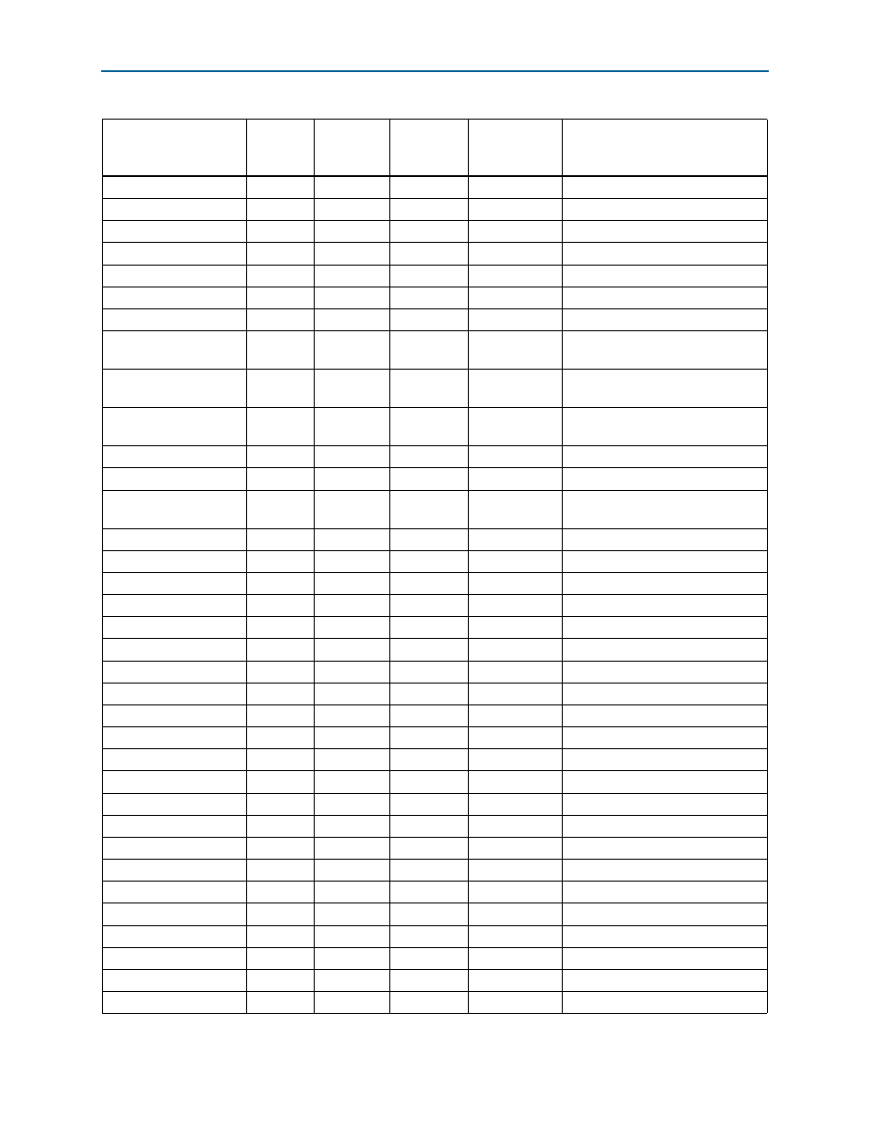
Table 2–5. MAX II CPLD EPM2210 System Controller Device (U10) Pin-Out (Part 2 of 5)
Schematic Signal Name
I/O
Standard
EPM2210
Pin Number
Stratix IV E
Device
Pin Number
Other
Connections
Description