Altera Stratix IV E FPGA Development Board User Manual
Page 11
Chapter 2: Board Components
2–3
Board Overview
May 2011
Altera Corporation
Stratix IV E FPGA Development Board Reference Manual
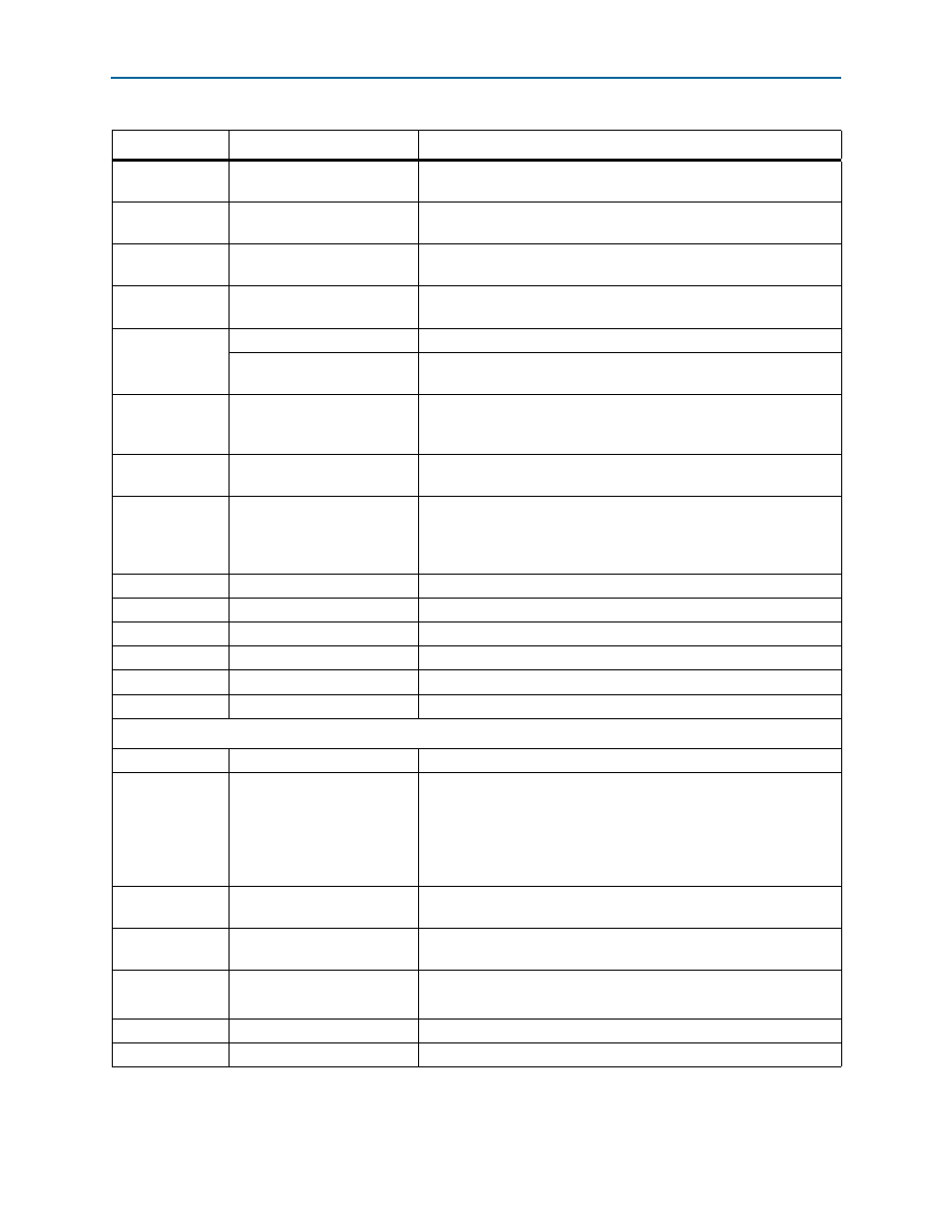
J15
HSMC Port A JTAG header
Place a shunt on this header to include the HSMC port A in the JTAG
chain.
J5
HSMC Port B JTAG header
Place a shunt on this header to include the HSMC port B in the JTAG
chain.
J10
MAX II JTAG header
Place a shunt on this header to include the MAX II CPLD EPM2210
System Controller in the JTAG chain.
SW1
Clock enable DIP switch
Enables the oscillators when the switch is ON (positioned on the left
side of the switch).
SW2
MAX II DIP switch
MAX II user DIP switches.
66 MHz oscillator select
Selects the on board oscillator when driven low and selects the
differential SMA inputs when driven high.
SW5
Rotary switch
Selects factory or user FPGA image to load on power up. After power
up, this switch selects the power rail monitored from among a total of
12 rails.
D7-D12
Ethernet LEDs
Illuminates to show the connection speed as well as transmit or
receive activity.
D15, D17-D20
MAX II LEDs
Illuminates when the MAX II CPLD EPM2210 System Controller is
actively configuring the FPGA. The LED types include MAX_EMB
(labeled as USER_1 on the board), MAX_LOAD, MAX_FACTORY, MAX_PB
(labeled as USER_2 on the board), and MAX_ERROR.
D21
Power LED
Illuminates when power is present.
D22
Configuration done LED
Illuminates when the FPGA is configured.
D13, D14
HSMC port A status LEDs
You can configure these LEDs to indicate transmit or receive activity.
D16
HSMC port A present LED
Illuminates when a daughtercard is plugged into the HSMC port A.
D3, D4
HSMC port B status LEDs
You can configure these LEDs to indicate transmit or receive activity.
D5
HSMC port B present LED
Illuminates when a daughtercard is plugged into the HSMC port B.
Clock Circuitry
X2
100 MHz oscillator
100.0 MHz crystal oscillator to the FPGA.
X3
66 MHz oscillator
66.6 MHz crystal oscillator with a single-ended input to the LVDS clock
buffer (U22). This oscillator is also MUXed with the differential SMA
clock inputs (J13 and J14) based on the CLK66_SEL input. The
CLK66_SEL
signal needs to be set to '0' on SW2 to enable the
oscillator clock source. Two LVDS clocks are output from the clock
buffer to the FPGA.
X4
125 MHz oscillator
125.000 MHz crystal oscillator to the LVDS clock buffer. Two LVDS
clocks are output from the clock buffer to the FPGA.
X5
50 MHz oscillator
50 MHz single-ended oscillator to the FPGA and MAX II CPLD
EPM2210 System Controller.
Y2
100 MHz oscillator
(for MAX II CPLD)
100 MHz single-ended dedicated clock oscillator to the MAX II CPLD
EPM2210 System Controller.
J17
Clock input SMAs
Drives LVPECL-compatible clock inputs into the FPGA.
J16
Clock output SMA
Drives out 2.5-V CMOS clock output from the FPGA.
Table 2–1. Stratix IV E FPGA Development Board Components (Part 2 of 4)
Board Reference
Type
Description