Altera Cyclone IV GX FPGA Development Board User Manual
Page 11
Chapter 2: Board Components
2–3
Board Overview
May 2013
Altera Corporation
Cyclone IV GX FPGA Development Board
Reference Manual
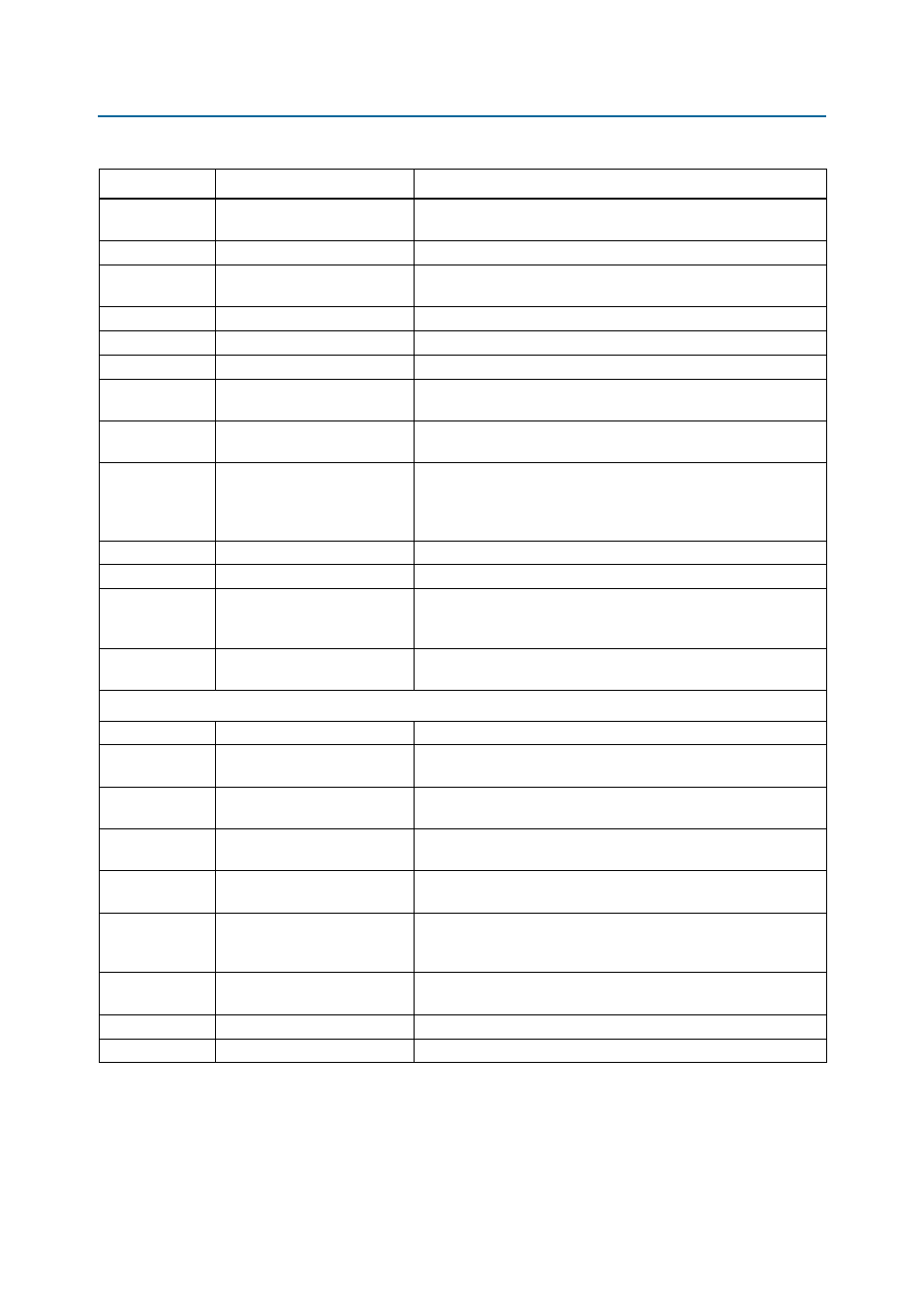
D17
Load LED
Illuminates when the MAX II CPLD EPM2210 System Controller is
actively configuring the FPGA.
D18
Error LED
Illuminates when the FPGA configuration from flash memory fails.
D24–D27, D30,
D31
Ethernet LEDs
Shows the connection speed as well as transmit or receive activity.
D11
Power LED
Illuminates when 14-V – 20-V DC power is present.
D28
PCIe x4 LED
You can configure this LED to illuminate when PCIe is in x4 mode.
D29
PCIe x1 LED
You can configure these LEDs to illuminate when PCIe is in x1 mode.
SW4
PCIe DIP switch
Controls the PCIe lane width (connecting prsnt pins together on the
PCIe edge connector) or disables the embedded USB-Blaster.
SW5
JTAG chain select DIP switch
Enables and disables devices in the JTAG chain. The switch is located
under the character LCD.
SW1
Board settings DIP switch
Controls the Max II CPLD EPM2210 System Controller functions
such as enabling the 125-MHz clock or programmable clock, as well
as selection between the SMA clock input or the programmable clock
for buffer multiplexer.
S5
System reset push button
Press to reset the MAX II CPLD EPM2210 System Controller.
S6
CPU reset push button
Press to reset the FPGA logic.
S7
Program select push button
Toggles the LEDs which selects the program image that loads either
from the flash memory (FPP mode) or the EPCS device (active serial
mode) to the FPGA.
S8
Program load push button
Configure the FGPA from flash memory based on the program select
LEDs setting.
Clock Circuitry
X2
125-MHz oscillator
125-MHz crystal oscillator for general use such as memories.
X3
50-MHz oscillator
50-MHz crystal oscillator for configuration purpose. This oscillator is
located at the bottom of the board.
X5
25-MHz oscillator
25-MHz crystal oscillator for 10 Gigabit Ethernet. This oscillator is
located at the bottom of the board.
Y2
6-MHz oscillator
6-MHz crystal oscillator for USB PHY. This oscillator is located at the
bottom of the board.
X1
24-MHz oscillator
24-MHz crystal oscillator for USB PHY. This oscillator is located at
the bottom of the board.
X4
Programmable oscillator
Programmable oscillator for PCIe or general use such as memories.
Multiplexed with CLKIN_SMA_P/N signals based on CLK_SEL switch
value.
J11, J12
Clock input SMA
Drive LVPECL-compatible clock input into the clock multiplexer
buffer.
J10
Single-ended clock input
1.8-V single-ended clock input.
J9
Clock output SMA
Drives out 2.5-V CMOS clock output from the FPGA.
Table 2–1. Cyclone IV GX FPGA Development Board Components (Part 2 of 3)
Board Reference
Type
Description