Memory, Ddr2 sdram, Memory –38 – Altera Cyclone IV GX FPGA Development Board User Manual
Page 46: Ddr2 sdram –38
2–38
Chapter 2: Board Components
Memory
Cyclone IV GX FPGA Development Board
May 2013
Altera Corporation
Reference Manual
lists the HSMC connector component reference and manufacturing
information.
Memory
This section describes the board's memory interface support and also their signal
names, types, and connectivity relative to the Cyclone IV GX device. The board has
the following memory interfaces:
■
DDR2 SDRAM
■
SSRAM
■
Flash
DDR2 SDRAM
There are four DDR2 devices, providing 256 MB of memory for each on-board DDR2
SDRAM device. Each device interface has a 16-bit data bus, which can be configured
to run individually or together as a 32-bit data bus.
Two DDR2 devices are pinned out to FPGA bank 3 and 4 (bottom port) while another
two are pinned out to FPGA bank 7 and 8 (top port). These memory interfaces are
designed to run at a maximum frequency of 167 MHz for a maximum theoretical
bandwidth of over 10.6 Gbps. The internal bus in the FPGA is typically 2 or 4 times
the width at full rate or half rate respectively. For example, a 167 MHz 16-bit interface
becomes a 83.5 MHz 64-bit bus.
HSMB_TX_N1
XCVR_TX_N1
Y3
HSMB_TX_N2
XCVR_TX_N2
V3
HSMB_TX_N3
XCVR_TX_N3
T3
HSMB_TX_P0
XCVR_TX_P0
AB4
HSMB_TX_P1
XCVR_TX_P1
Y4
HSMB_TX_P2
XCVR_TX_P2
V4
HSMB_TX_P3
XCVR_TX_P3
T4
Table 2–35. HSMC Port B Transceiver and PCIe Signals (Part 2 of 2)
HSMC Port B Transceiver
Signal
PCIe Signal
Cyclone IV GX Device Pin
Number
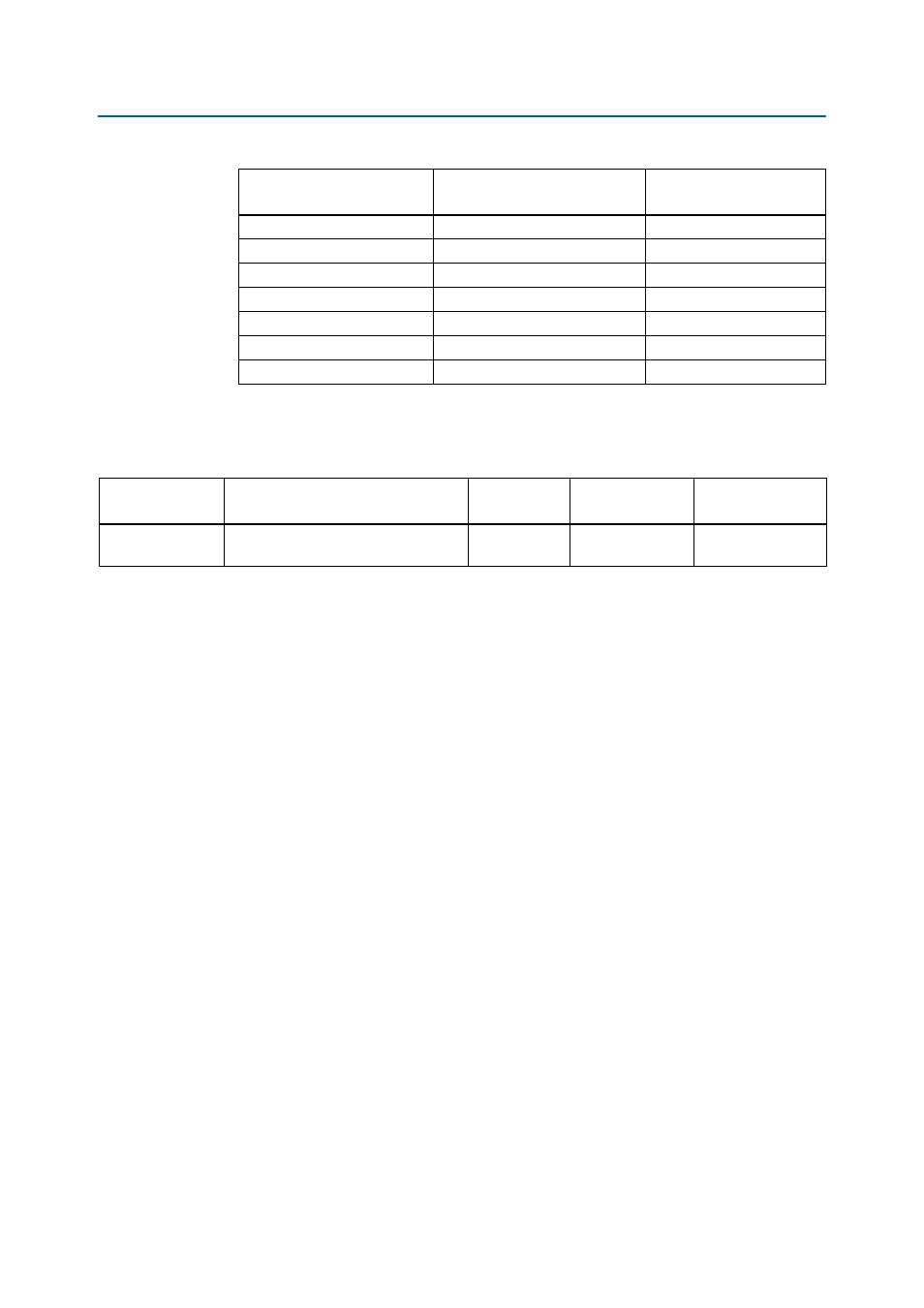
Table 2–36. HSMC Connector Component Reference and Manufacturing Information
Board Reference
Description
Manufacturer
Manufacturing
Part Number
Manufacturer
Website
J1 and J2
HSMC, custom version of QSH-DP
family high-speed socket.
Samtec
ASP-122953-01