Altera Cyclone IV GX FPGA Development Board User Manual
Page 33
Chapter 2: Board Components
2–25
General User Input/Output
May 2013
Altera Corporation
Cyclone IV GX FPGA Development Board
Reference Manual
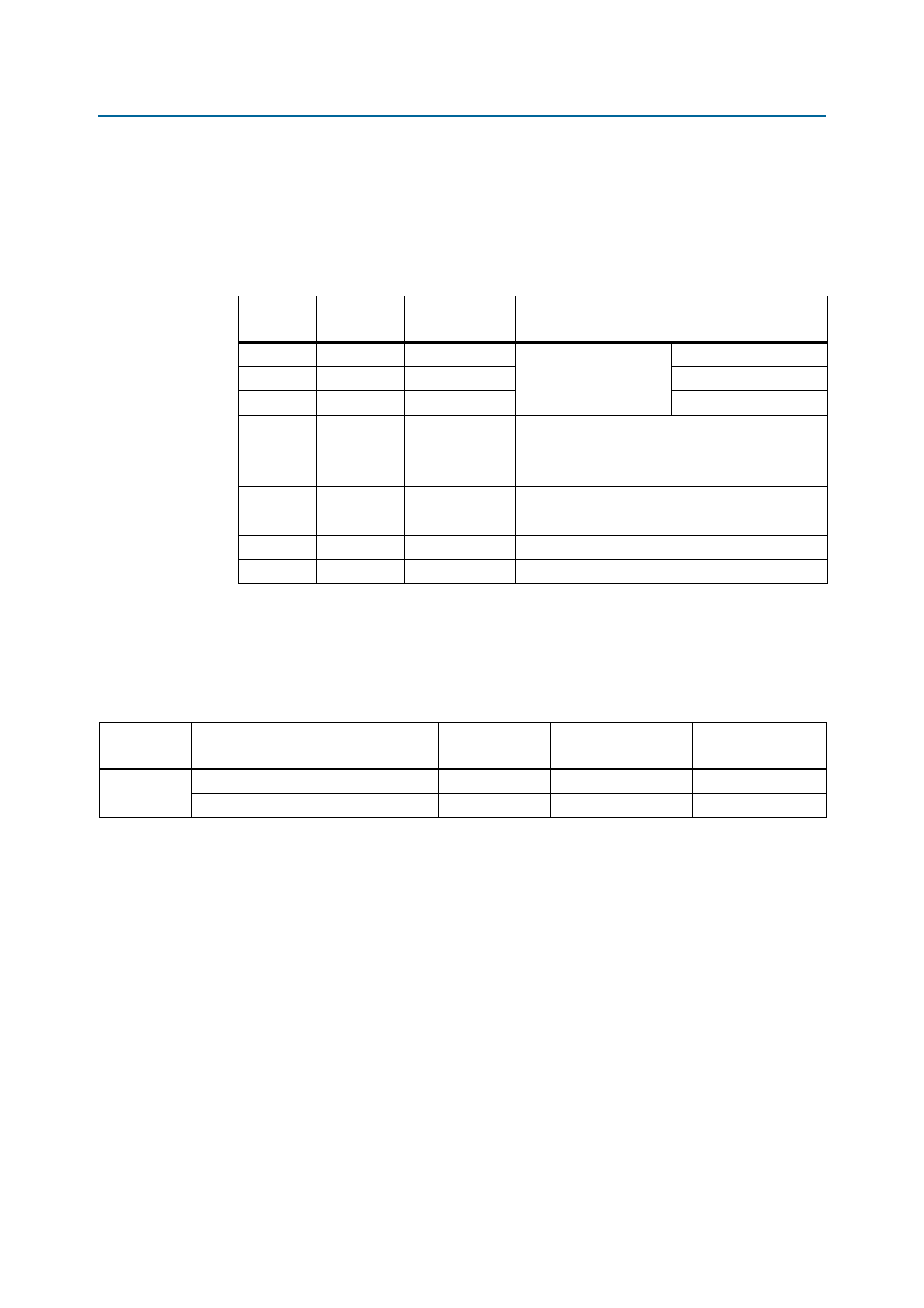
shows the LCD pin definitions, and is an excerpt from the Lumex data
sheet.
f
For more information such as timing, character maps, interface guidelines, and other
related documentation, visi
1
The particular model used does not have a backlight and the LCD drive pin is not
connected to the power pin for maximum pixel drive.
lists the LCD component references and the manufacturing information.
Table 2–27. LCD Pin Definitions and Functions
Pin
Number
Symbol
Level
Function
1
V
DD
—
Power supply
5 V
2
V
SS
—
GND (0 V)
3
V
0
—
For LCD drive
4
RS
H/L
Register select signal
H: Data input
L: Instruction input
5
R/W
H/L
H: Data read (module to MPU)
L: Data write (MPU to module)
6
E
H, H to L
Enable
7–14
DB0–DB7
H/L
Data bus, software selectable 4-bit or 8-bit mode
Table 2–28. LCD Component References and Manufacturing Information
Board
Reference
Description
Manufacturer
Manufacturer
Part Number
Manufacturer
Website
J13
2×7 pin, 100 mil, vertical header
Samtec
TSM-107-07-G-D
2×16 character display, 5×8 dot matrix
Lumex Inc.
LCM-S01602DSR/C