Altera Cyclone IV GX FPGA Development Board User Manual
Page 45
Chapter 2: Board Components
2–37
Components and Transceiver Interfaces
May 2013
Altera Corporation
Cyclone IV GX FPGA Development Board
Reference Manual
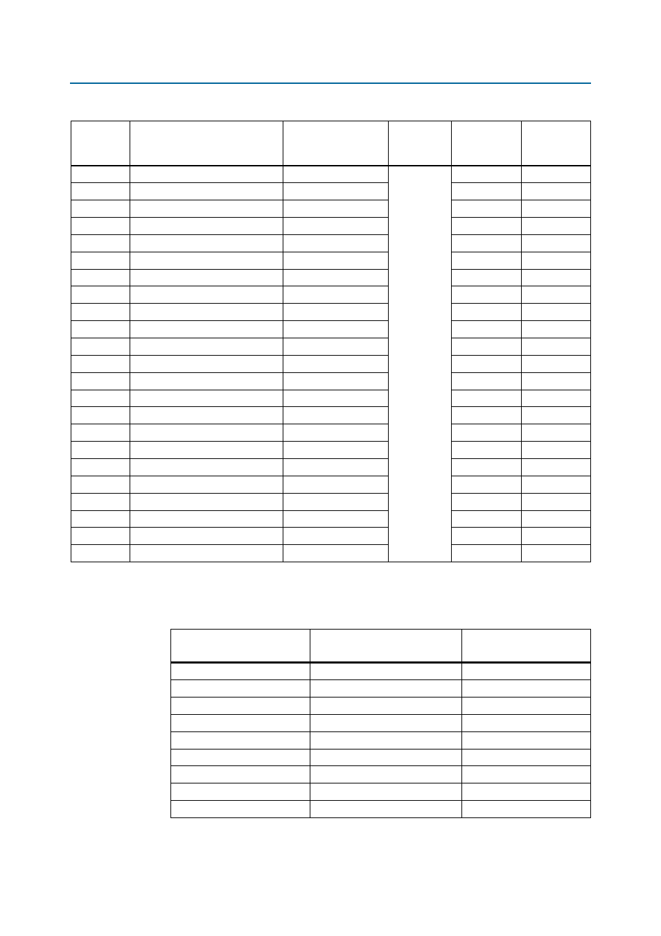
lists the signals that multiplex between the PCIe and the HSMB
transceivers.
—
—
HSMB_RX_D_P16
1.8-V
D3
U28.3
—
—
HSMB_TX_D_N6
AH28
U36.8
—
—
HSMB_TX_D_N7
AJ27
U36.6
—
—
HSMB_TX_D_N8
AH22
U35.7
—
—
HSMB_TX_D_N10
AH21
U35.3
—
—
HSMB_TX_D_N11
AF7
U29.7
—
—
HSMB_TX_D_N12
AF9
U29.6
—
—
HSMB_TX_D_N13
AJ21
U35.2
—
—
HSMB_TX_D_N14
AF22
U35.5
—
—
HSMB_TX_D_N15
AK6
U28.2
—
—
HSMB_TX_D_N16
AH25
U36.3
—
—
HSMB_TX_D_P6
AG28
U36.9
—
—
HSMB_TX_D_P7
AJ28
U36.7
—
—
HSMB_TX_D_P8
AG26
U36.5
—
—
HSMB_TX_D_P9
AJ22
U35.4
—
—
HSMB_TX_D_P10
AH26
U36.4
—
—
HSMB_TX_D_P11
AK21
U29.8
—
—
HSMB_TX_D_P12
AE23
U36.2
—
—
HSMB_TX_D_P13
AF10
U29.5
—
—
HSMB_TX_D_P14
AK24
U35.8
—
—
HSMB_TX_D_P15
AD22
U35.6
—
—
HSMB_TX_D_P16
AF25
U35.9
—
—
HSMBT_CLK_IN0
AJ16
U30.3
Table 2–34. HSMC Port B Pin Assignments, Schematic Signal Names, and Functions (Part 5 of 5)
Board
Reference
Description
Schematic Signal
Name
I/O Standard
Cyclone IV GX
Device
Pin Number
Other
Connections
Table 2–35. HSMC Port B Transceiver and PCIe Signals (Part 1 of 2)
HSMC Port B Transceiver
Signal
PCIe Signal
Cyclone IV GX Device Pin
Number
HSMB_RX_N0
XCVR_RX_N0
AC1
HSMB_RX_N1
XCVR_RX_N1
AA1
HSMB_RX_N2
XCVR_RX_N2
W1
HSMB_RX_N3
XCVR_RX_N3
U1
HSMB_RX_P0
XCVR_RX_P0
AC2
HSMB_RX_P1 XCVR_RX_P1
AA2
HSMB_RX_P2
XCVR_RX_P2
W2
HSMB_RX_P3
XCVR_RX_P3
U2
HSMB_TX_N0
XCVR_TX_N0
AB3