I/o resources, I/o resources –6 – Altera Cyclone IV GX FPGA Development Board User Manual
Page 14
2–6
Chapter 2: Board Components
Featured Device: Cyclone IV GX Device
Cyclone IV GX FPGA Development Board
May 2013
Altera Corporation
Reference Manual
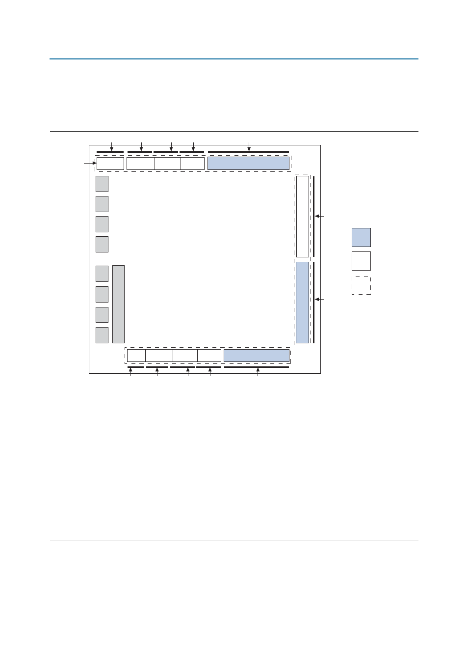
I/O Resources
illustrates the bank organization and I/O count for the EP4CGX150DF31
device in the 896-pin FBGA package.
Figure 2–2. EP4CGX150DF31 Device I/O Bank Diagram
Notes to
(1) This is a top view of the silicon die. For exact pin locations, refer to the pin list and the Quartus II software.
(2) True differential (PPDS, LVDS, mini-LVDS, and RSDS I/O standards) outputs are supported in row I/O banks 5 and 6 only. External resistors are
needed for the differential outputs in column I/O banks.
(3) The LVPECL I/O standard is only supported on clock input pins. This I/O standard is not supported on output pins.
(4) The HSTL-12 Class II is supported in column I/O banks 4, 7, and 8.
(5) The differential SSTL-18 and SSTL-2, differential HSTL-18, and HSTL-15 I/O standards are supported only on clock input pins and phase-locked
loops (PLLs) output clock pins. PLL output clock pins do not support Class II interface type of differential SSTL-18, HSTL-18, HSTL-15, and
HSTL-12 I/O standards.
(6) The differential HSTL-12 I/O standard is only supported on clock input pins and PLL output clock pins. Differential HSTL-12 Class II is supported
only in column I/O banks 4, 7, and 8.
(7) BLVDS output uses two single-ended outputs with the second output programmed as inverted. BLVDS input uses the LVDS input buffer.
(8) The PCI-X I/O standard does not meet the IV curve requirement at the linear region.
(9) The OCT block is located in the shaded banks 4, 5, and 7.
(10) The dedicated clock input I/O banks 3A, 3B, 8A, and 8B can be used either for HSSI input reference clock pins or clock input pins.
(11) Single-ended clock input support is available for dedicated clock input I/O banks 3B and 8B.
Right, Top, and Bottom Banks Support:
3.3-V LVTTL/LVCMOS
3.0-V LVTTL/LVCMOS
2.5-V LVTTL/LVCMOS
1.8-V LVTTL/LVCMOS
1.5-V LVCMOS
1.2-V LVCMOS
PPDS
LVDS
RSDS
mini-LVDS
Bus LVDS (7)
LVPECL (3)
SSTL-2 class I and II
SSTL-18 CLass I and II
HSTL-18 Class I and II
HSTL-15 Class I and II
HSTL-12 Class I and II (4)
Differential SSTL-2 (5)
Differential SSTL-18 (5)
Differential HSTL-18 (5)
Differential HSTL-15 (5)
Differential HSTL-12 (6)
3.0-V PCI/PCI-X (8)
VCCIO9
Configuration
pins
Config
pins
VCCIO8 VCC_CLKIN8A
VCC_CLKIN3A
VCCIO7
VCCIO6
VCCIO5
VCCIO4
VCCIO3
I/O Bank 9
I/O Bank 7
I/O Bank 4
I/O Bank 5
PCIe hard IP x1, x2, and x4
I/O Bank 6
VCC_CLKIN8B
VCCIO3
VCC_CLKIN3B
Ch0
Ch1
Ch2
GXBL0
Ch3
Ch0
Ch1
Ch2
GXBL1
Ch3
I/O bank with
calibration block
I/O bank without
calibration block
Calibration block
coverage
I/O Bank 8
I/O Bank
8A (10)
I/O Bank 8B
(10), (11)
I/O Bank 3
I/O Bank
3A (10)
I/O Bank 3B
(10), (11)