Altera Cyclone IV GX FPGA Development Board User Manual
Page 12
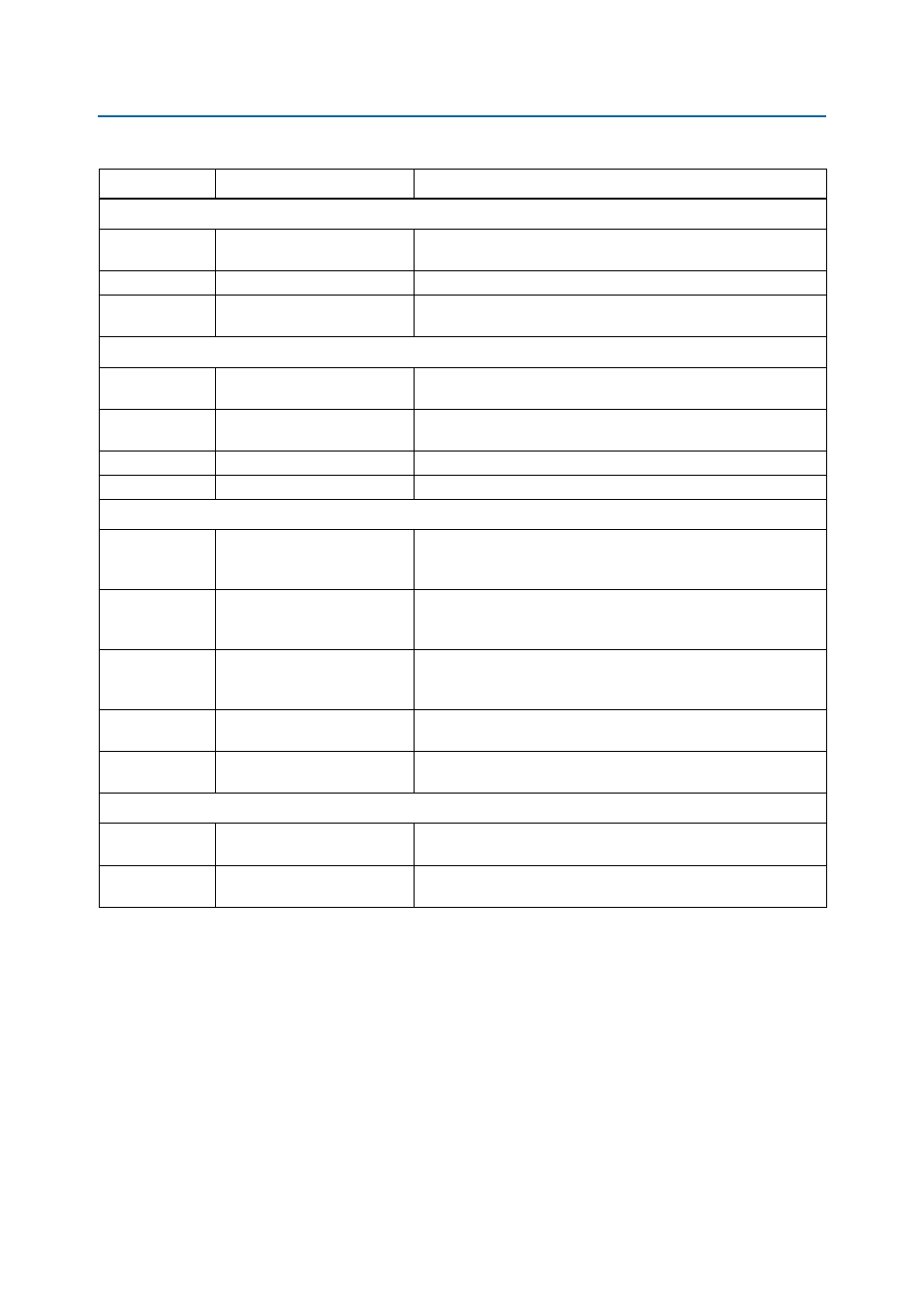
2–4
Chapter 2: Board Components
Board Overview
Cyclone IV GX FPGA Development Board
May 2013
Altera Corporation
Reference Manual
General User Input/Output
D7–D10,
D12–D15
User LEDs
Eight user LEDs. Illuminates when driven low.
S1–S4
User push buttons
Four user push buttons. Driven low when pressed.
J13
Character LCD
Connector which interfaces to the provided 16 character × 2 line LCD
module.
Memory Devices
U44
SSRAM x18 memory
Standard synchronous RAM which provides a 72-Mbit (Mb) SSRAM
port. This SSRAM is located at the bottom of the board.
U6
Flash x64 memory
Synchronous burst mode flash device which provides a 256-Mb
non-volatile memory port.
U8, U15
DDR2 x32 SDRAM A
Two 16-bit memory device.
U17, U19
DDR2 x32 SDRAM B
Two 16-bit memory device.
Components Interfaces
J7
RJ-45 connector
Provides 10/100/1000 BASE-T Ethernet connection via a Marvell
88E1111 PHY and the FPGA-based Altera Triple Speed Ethernet
MegaCore function in RGMII mode.
U21
Gigabit Ethernet
A Marvell 88E1111 PHY device for 10/100/1000 BASE-T Ethernet
connection. The device is an auto-negotiating Ethernet PHY with an
RGMII interface to the FPGA.
J14
PCIe edge connector
Interfaces to a PCIe root port such as an appropriate PC
motherboard. Made of gold-plated edge fingers for up to ×4 signaling
in Gen1 mode.
J1
HSMC port A
Provides eight transceiver channels and 84 CMOS or 17 LVDS
channels per the HSMC specification.
J2
HSMC port B
Provides eight transceiver channels and 84 CMOS channels per the
HSMC specification.
Power Supply
J5
DC input jack
Accepts a 16-V DC power supply. Do not use this input jack while the
board is plugged into a PCIe slot.
SW3
Power switch
Switch to power on or off the board when power is supplied from the
DC input jack.
Table 2–1. Cyclone IV GX FPGA Development Board Components (Part 3 of 3)
Board Reference
Type
Description