Ddr2 sdram top port, Ddr2 sdram top port –39 – Altera Cyclone IV GX FPGA Development Board User Manual
Page 47
Chapter 2: Board Components
2–39
Memory
May 2013
Altera Corporation
Cyclone IV GX FPGA Development Board
Reference Manual
DDR2 SDRAM Top Port
The DDR2 SDRAM top port consists of two DDR2 devices (U8 and U15).
lists the DDR2 top port pin assignments, signal names, and its functions. The signal
names and types are relative to the Cyclone IV GX device in terms of I/O setting and
direction.
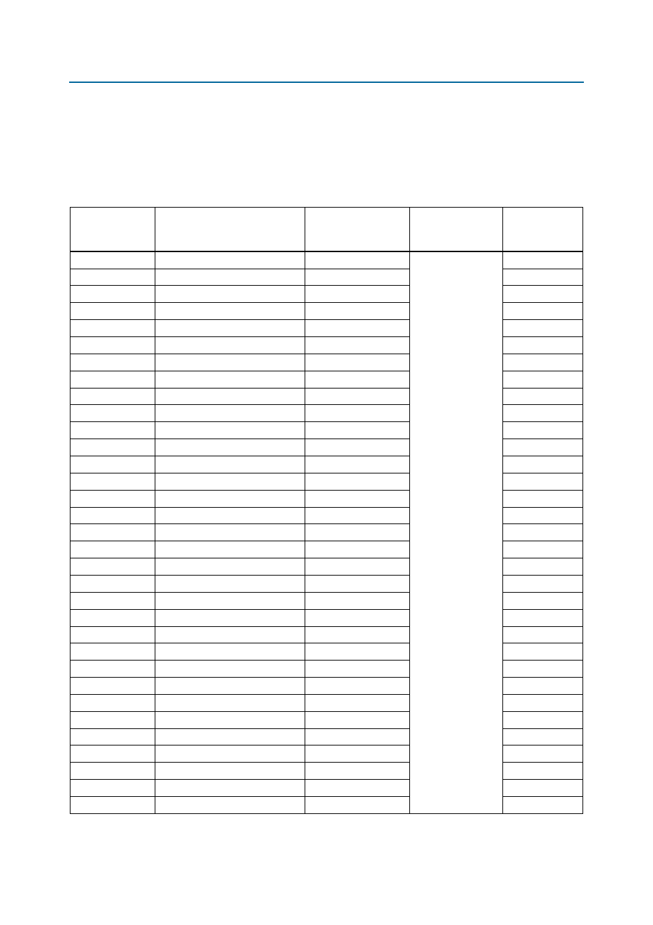
Table 2–37. DDR2 SDRAM Top Port Pin Assignments, Signal Names and Functions (Part 1 of 2)
Board Reference
Description
Schematic Signal
Name
I/O Standard
Cyclone IV GX
Device
Pin Number
U8.R2, U15.R2
Address bus
DDR2A_A12
1.8-V SSTL Class I
F21
U8.P7, U15.P7
Address bus
DDR2A_A11
G18
U8.M2, U15.M2
Address bus
DDR2A_A10
C20
U8.P3, U15.P3
Address bus
DDR2A_A9
F20
U8.P8, U15.P8
Address bus
DDR2A_A8
K17
U8.P2, U15.P2
Address bus
DDR2A_A7
B22
U8.N7, U15.N7
Address bus
DDR2A_A6
F17
U8.N3, U15.N3
Address bus
DDR2A_A5
B21
U8.N8, U15.N8
Address bus
DDR2A_A4
F18
U8.N2, U15.N2
Address bus
DDR2A_A3
A21
U8.M7, U15.M7
Address bus
DDR2A_A2
D17
U8.M3, U15.M3
Address bus
DDR2A_A1
C19
U8.M8, U15.M8
Address bus
DDR2A_A0
D18
U8.L3, U15.L3
Bank address bus
DDR2A_BA1
B19
U8.L2, U15.L2
Bank address bus
DDR2A_BA0
A20
U8.K7, U15.K7
Row address select
DDR2A_RASn
B18
U8.L7, U15.L7
Column address select
DDR2A_CASn
A16
U8.L8, U15.L8
Chip select
DDR2A_CSn
D20
U8.K3, U15.K3
Write enable
DDR2A_WEn
A18
U8.K9, U15.K9
Termination enable
DDR2A_ODT
C17
U8.K2, U15.K2
Clock enable
DDR2A_CKE
A19
U8.J8, U15.J8
Clock P
DDR2A_CLK_P
D23
U8.K8, U15.K8
Clock N
DDR2A_CLK_N
C23
U8.G8,
Data bus byte lane 0
DDR2A_DQ0
G23
U8.G2
Data bus byte lane 0
DDR2A_DQ1
D28
U8.H7
Data bus byte lane 0
DDR2A_DQ2
G24
U8.H3
Data bus byte lane 0
DDR2A_DQ3
C28
U8.H1
Data bus byte lane 0
DDR2A_DQ4
H24
U8.H9
Data bus byte lane 0
DDR2A_DQ5
F23
U8.F1
Data bus byte lane 0
DDR2A_DQ6
B30
U8.F9
Data bus byte lane 0
DDR2A_DQ7
F22
U8.F3
Write mask byte lane 0
DDR2A_DM0
G22
U8.F7
Data strobe byte lane 0
DDR2A_DQS0
A29