Altera Cyclone IV GX FPGA Development Board User Manual
Page 48
2–40
Chapter 2: Board Components
Memory
Cyclone IV GX FPGA Development Board
May 2013
Altera Corporation
Reference Manual
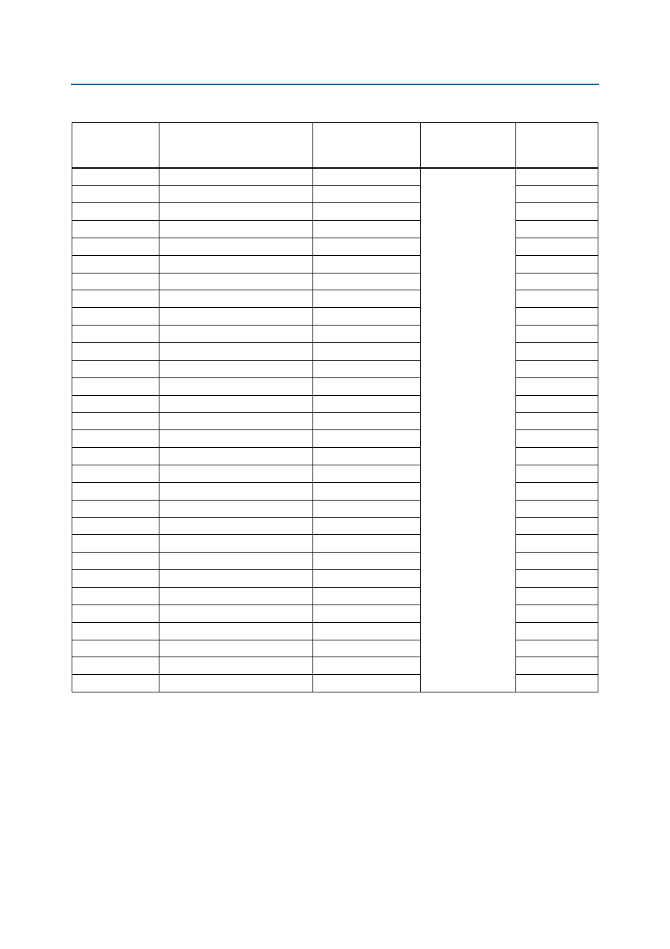
U8.C8
Data bus byte lane 1
DDR2A_DQ8
1.8-V SSTL Class I
D22
U8.C2
Data bus byte lane 1
DDR2A_DQ9
A26
U8.D7
Data bus byte lane 1
DDR2A_DQ10
E24
U8.D3
Data bus byte lane 1
DDR2A_DQ11
D26
U8.D1
Data bus byte lane 1
DDR2A_DQ12
B28
U8.D9
Data bus byte lane 1
DDR2A_DQ13
D21
U8.B1
Data bus byte lane 1
DDR2A_DQ14
B27
U8.B9
Data bus byte lane 1
DDR2A_DQ15
F19
U8.B3
Write mask byte lane 1
DDR2A_DM1
A24
U8.B7
Data strobe byte lane 1
DDR2A_DQS1
G17
U15.G8
Data bus byte lane 2
DDR2A_DQ16
E19
U15.G2
Data bus byte lane 2
DDR2A_DQ17
D19
U15.H7
Data bus byte lane 2
DDR2A_DQ18
C18
U15.H3
Data bus byte lane 2
DDR2A_DQ19
A17
U15.H1
Data bus byte lane 2
DDR2A_DQ20
A23
U15.H9
Data bus byte lane 2
DDR2A_DQ21
E18
U15.F1
Data bus byte lane 2
DDR2A_DQ22
C22
U15.F9
Data bus byte lane 2
DDR2A_DQ23
K18
U15.F3
Write mask byte lane 2
DDR2A_DM2
B16
U15.F7
Data strobe byte lane 2
DDR2A_DQS2
K19
U15.C8
Data bus byte lane 3
DDR2A_DQ24
A13
U15.C2
Data bus byte lane 3
DDR2A_DQ25
C14
U15.D7
Data bus byte lane 3
DDR2A_DQ26
A12
U15.D3
Data bus byte lane 3
DDR2A_DQ27
A14
U15.D1
Data bus byte lane 3
DDR2A_DQ28
D16
U15.D9
Data bus byte lane 3
DDR2A_DQ29
F13
U15.B1
Data bus byte lane 3
DDR2A_DQ30
D15
U15.B9
Data bus byte lane 3
DDR2A_DQ31
F12
U15.B3
Write mask byte lane 3
DDR2A_DM3
A8
U15.B7
Data strobe byte lane 3
DDR2A_DQS3
C16
Table 2–37. DDR2 SDRAM Top Port Pin Assignments, Signal Names and Functions (Part 2 of 2)
Board Reference
Description
Schematic Signal
Name
I/O Standard
Cyclone IV GX
Device
Pin Number