Altera Cyclone IV GX FPGA Development Board User Manual
Page 35
Chapter 2: Board Components
2–27
Components and Transceiver Interfaces
May 2013
Altera Corporation
Cyclone IV GX FPGA Development Board
Reference Manual
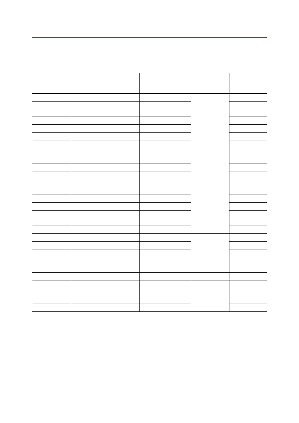
summarizes the PCIe pin assignments. The signal names and directions are
relative to the Cyclone IV GX FPGA.
Table 2–29. PCIe Pin Assignments, Schematic Signal Names, and Functions
Board Reference
Description
Schematic Signal Name
I/O Standard
Cyclone IV GX
Device
Pin Number
J14.A16
Add-in card transmit bus
PCIE_TX_P0
1.5-V PCML
J14.A17
Add-in card transmit bus
PCIE_TX_N0
J14.A21
Add-in card transmit bus
PCIE_TX_P1
J14.A22
Add-in card transmit bus
PCIE_TX_N1
J14.A25
Add-in card transmit bus
PCIE_TX_P2
J14.A26
Add-in card transmit bus
PCIE_TX_N2
J14.A29
Add-in card transmit bus
PCIE_TX_P3
T4
J14.A30
Add-in card transmit bus
PCIE_TX_N3
T3
J14.B14
Add-in card receive bus
PCIE_RX_P0
J14.B15
Add-in card receive bus
PCIE_RX_N0
J14.B19
Add-in card receive bus
PCIE_RX_P1
J14.B20
Add-in card receive bus
PCIE_RX_N1
J14.B23
Add-in card receive bus
PCIE_RX_P2
J14.B24
Add-in card receive bus
PCIE_RX_N2
J14.B27
Add-in card receive bus
PCIE_RX_P3
U2
J14.B28
Add-in card receive bus
PCIE_RX_N3
U1
J14.A13
Motherboard reference clock
PCIE_REFCLK_P
HCSL
V15
J14.A14
Motherboard reference clock
PCIE_REFCLK_N
W15
J14.A11
Reset
PCIE_T_PERSTn
LVTTL
A7
J14.B5
SMB clock
PCIE_T_SMBCLK
F15
J14.B6
SMB data
PCIE_T_SMBDAT
E12
J14.B11
Wake signal
PCIE_WAKEn_R
—
J14.B17
x1 Present
PCIE_PRSNT2n_x1
—
—
J14.B31
x4 Present
PCIE_PRSNT2n_x4
—
—
J14.A5
Motherboard TCK
PCIE_JTAG_TCK
3.3-V
—
J14.A6
Motherboard TDI
PCIE_JTAG_TDI
—
J14.A7
Motherboard TDO
PCIE_JTAG_TDO
—
J14.A8
Motherboard TMS
PCIE_JTAG_TMS
—
Notes to
:
(1) This signal is multiplexed with the signal on HSMC port B interface.
(2) The Quartus II version 10.1sp1 and newer only support an I/O standard of 1.5-V PCML for the PCI Express transmitter as stated in Altera’s
knowledge base webpage—solution ID