Development board block diagram, Development board block diagram –3 – Altera Cyclone IV GX FPGA Development Board User Manual
Page 7
Chapter 1: Overview
1–3
Development Board Block Diagram
May 2013
Altera Corporation
Cyclone IV GX FPGA Development Board
Reference Manual
■
Power supply
■
16-V DC input
■
2.5-mm barrel jack for DC power input
■
On/Off slide power switch
■
On-Board power measurement circuitry
■
20-W per HSMC interface
■
Mechanical
■
PCIe small form factor board
■
Bench-top operation
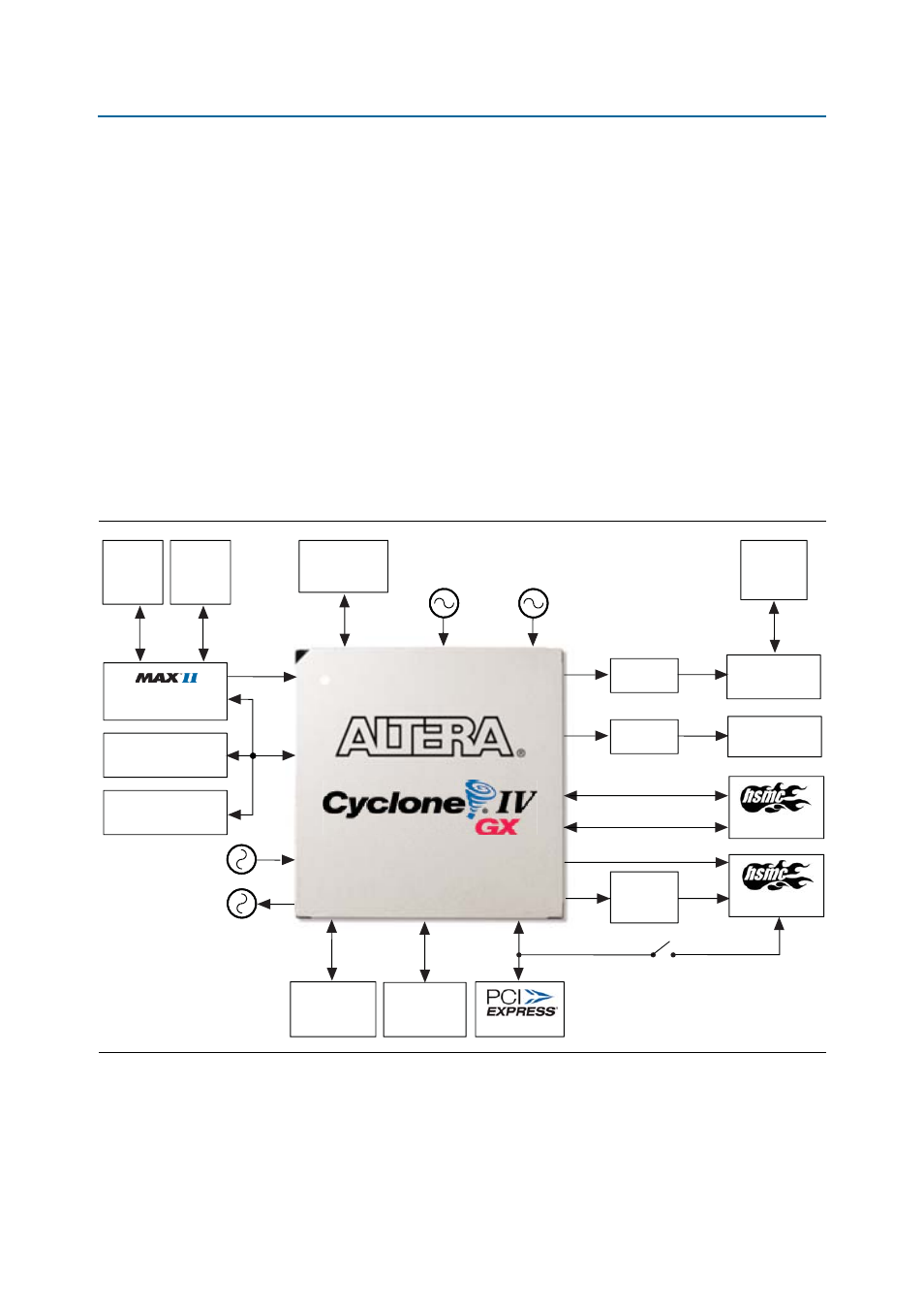
Development Board Block Diagram
shows the block diagram of the Cyclone IV GX FPGA development board.
Figure 1–1. Cyclone IV GX FPGA Development Board Block Diagram
EP4CGX150DF31
XCVR x4
10/100/1000
Ethernet RGMII
Translator
User LEDs
Push-Button,
Switches
14-pin LCD
Header
CPLD
(x18)
64 MB Flash
(x16)
4 MB SSRAM
(x18)
RJ45
Jack
Power
Measure
1.8 V
CMOS
1.8 V
CMOS
LVDS
1.8 V
2.5 V
Port B
USB
Blaster
100 MHz XTAL
SMA Input
125 MHz XTAL
32 MB DDR2
(x32)
SMA Output
1.8 V
HSTL
32 MB DDR2
(x32)
Translator
Port A
Translator
For TX/RX
[8:16]
1.8 V
XCVR x4
2.5 V
1.8 V
2.5 V
1.8 V
x4 Edge
XCVR x4
2.5 V (For TX/RX [0:7])