Altera Cyclone IV GX FPGA Development Board User Manual
Page 16
2–8
Chapter 2: Board Components
MAX II CPLD EPM2210 System Controller
Cyclone IV GX FPGA Development Board
May 2013
Altera Corporation
Reference Manual
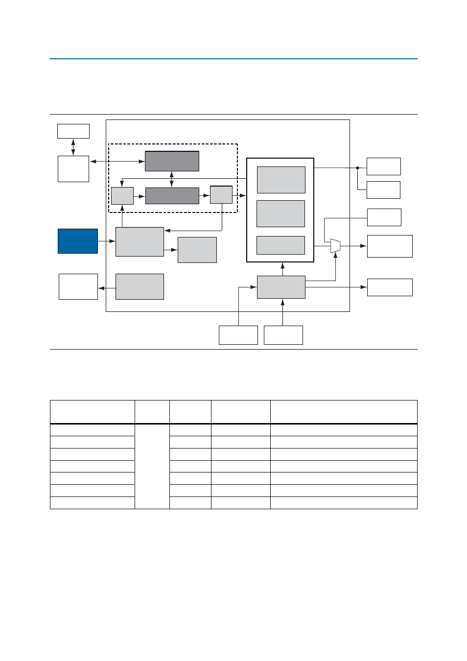
illustrates the MAX II CPLD EPM2210 System Controller's functionality
and external circuit connections as a block diagram.
lists the I/O signals present on the MAX
II CPLD EPM2210 System
Controller. The signal names and functions are relative to the MAX
II device (U7).
Figure 2–3. MAX II CPLD EPM2210 System Controller Block Diagram
Information
Register
MAX II
Embedded
USB-Blaster
MAX II CPLD EPM2210 System Controller
Power
Calculations
SLD-HUB
PFL
Power
Measurement
Results
Virtual-JTAG
PC
EP4CGX150
EPCS
LTC2418
Controller
FLASH
Decoder
Encoder
JTAG Control
Control
Register
Clock
Controller
Programmable
Clock
Configuration State
Machine
User/Factory
DIP Switch
Configuration
Push Buttons
Configuration
Signals (GPIO on
MAX Device)
Configuration
Status LEDs
Table 2–5. MAX II CPLD EPM2210 System Controller Device Pin-Out (Part 1 of 4)
Schematic Signal Name
I/O
Standard
EPM2210
Pin Number
EP4CGX15BF14
Pin Number
Description
CLKA_EN
2.5-V
H3
—
125-MHz oscillator enable
CLKA_SDA
J1
—
125-MHz programming data
CLKA_SCL
H4
—
125-MHz programming clock
CLK125_EN
J2
—
125-MHz oscillator enable
CLKIN_50
H5
—
50-MHz oscillator
CLKIN_MAX_100
J5
—
MAX II clock input
FAN_CNTL
P2
—
Fan control