Digital lines chapter 6 – Remote Processing RPC-2350 User Manual
Page 35
DIGITAL LINES
CHAPTER 6
6-2
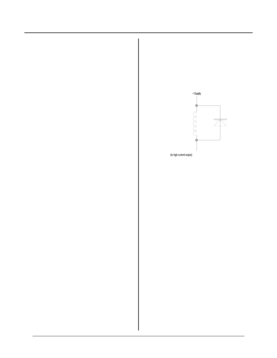
Figure 6-2 Inductive load protection
J3, port A is shared with the LCD character display port
J6. If you are using J6, then these 8 lines at J3 are not
available.
J3, port B is connected to a high current sink through
U20. See High current output later in this chapter. Two
lines are connected to the keypad port. They are active
only when scanning a 24 position keypad.
J3 port C is shared with the keypad port J5. If you are
using a keypa d through J5, the se 8 lines are not available
at J3.
Pull up resistors
Digital I/ O lines at J2 an d J3 are p ulled up to + 5 volts
through a 10K resistor pack.
These pull ups makes interfacing to switches and "open
collector" TTL devices easy . See "Inter facing to
Switches and other devices" below.
High cu rrent ou tput at J3
Eight lines at J3 can be used as high cur rent driver s.
These outputs switch loads to ground. Outputs are
controlled by Port B on the 82C55. Its address is 65.
Logic outputs from this port are inverted. That is, when
a 1 is writte n to the high cur rent por t, the o utput is
switched on and goes low.
The output driver chip, U 20, can be replaced w ith a DIP
shunt jumper so it is like the other lines at J3.
NOTE: Outputs at the high current lines are not
compa tible with TT L logic leve ls and should
not be used to drive other logic devices.
Each of the high current outputs can sink 100 mA.at
50V.
Two lines from the high curr ent port (Port B, 0 and 1)
are used wh en the keypad is scanning 24 keys. These
lines (at J3-8 and -10) may not be used for control
purposes.
WARNING:
External supplies using the high cu rrent outputs m ust
be tied to J3, pin 26 and NOT the power connector.
Failure to do so can produce a ground loop and
cause erratic operation.
The thermal time constant of U20 is very short, so the
numbe r of outputs th at are on a t any one tim e should
include those that overlap even for a few milliseconds.
Incandesc ent lamps h ave a " cold" c urre nt of 11 times its
operating current. Lamps requiring more than 50 mA.
should not be used.
Protection diodes m ust be used with inductive loads.
Refer to figure 6-2.
Do not pa rallel outputs f or higher drive. This could
result in damage since outputs do not share current
equally.
High current output at P2
The P2 term inal marked “ SWPW R” is a 2 Am p, 50V
F E T s w it c h t o g r o un d . O N r es is ta n ce is a bo u t 1 o hm .
I t i s i nt e nd e d t o s w it c h b a ck li gh t p o we r fo r th e L C D
graphics display. However , it can be used for any other
purpose.
The switch is contr olled by software as follow s:
OUT &E7,1
:’Turns on switch
OUT &E7,0
:’Turns off switch
The switch is turned OFF when only on a hardware reset
or wa tchdog time out.
Use the circuit in Figure 6-2 when switching inductive
loads.
Interfacing to an opto-module rack
J2 and J3 I/O lines interface to an MPS-8, 16, or 24
position opto m odule rac k. L ines not going to an opto
module connect to a screw terminal on the MPS-XX
series boards. This feature allows you to connect
s w it ch e s o r ot he r T T L t yp e de v ic e s t o t he d ig it al I/ O