Altera LVDS SERDES Transmitter / Receiver User Manual
Page 45
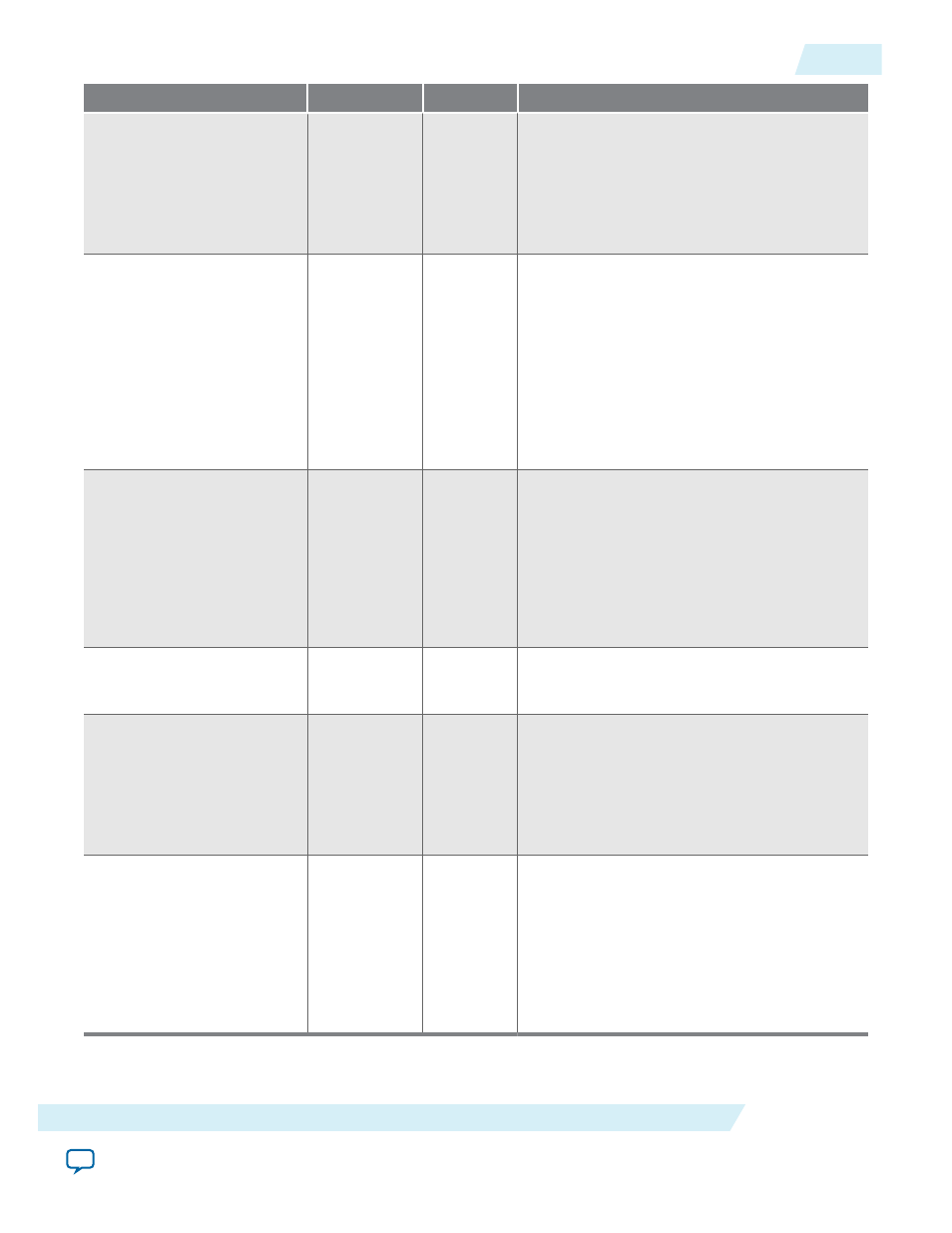
Port Name
Direction
Width (Bit)
Description
rx_cda_max
Output
n
Data re-alignment (bit slip) roll-over signal.
When high for one parallel clock cycle, this
signal indicates that the user-programmed
number of bits for the word boundary to roll-
over have been slipped. Indicates when the
next
rx_channel_data_align
pulse restores
the serial data latency back to 0.
rx_divfwdclk
Output
n
Parallel DPA clock to the FPGA fabric logic
array. The parallel receiver output data to the
FPGA fabric logic array is synchronous to this
clock in soft-CDR mode. This signal is not
available in non-DPA and DPA modes.
Divides and forwards the clock to the source
from the DPA block of the clock channel.
When the
enable_soft_cdr_mode
parameter
is set to
ON
, the
rx_divfwdclk
port is used.
When set to
ON
, the
rx_divfwdclk
port clocks
the synchronization registers.
rx_dpa_locked
Output
n
Indicates whether the channel is locked to
DPA mode. This signal only indicates an
initial DPA lock condition to the optimum
phase after power up or reset. This signal is
not deasserted if the DPA selects a new phase
out of the eight clock phases to sample the
received data. You must not use the
rx_dpa_
locked
signal to determine a DPA loss-of-
lock condition.
rx_locked
Output
1
Provides the LVDS PLL status. Stays high
when the PLL is locked to
rx_inclock
, and
stays low when the PLL fails to lock.
rx_out
Output
m
Receiver parallel data output. The data bus
width per channel is the same as the deseriali‐
zation factor (DF). The output data is
synchronous to the
rx_outclock
signal in
non-DPA and DPA modes. It is synchronous
to the
rx_divfwdclk
signal in soft-CDR
mode.
rx_outclock
Output
1
Parallel output clock from the receiver PLL.
The parallel data output from the receiver is
synchronous to this clock in non-DPA and
DPA modes. This port is not available when
you turn on the Use External PLL option in
the parameter editor. The FPGA fabric-
receiver interface clock must be driven by the
PLL instantiated through the PLL IP core
parameter editor.
UG-MF9504
2014.12.15
ALTLVDS_RX Ports
45
LVDS SERDES Transmitter/Receiver IP Cores User Guide
Altera Corporation