Dpa pll calibration, Dpa pll calibration in stratix iv es devices – Altera LVDS SERDES Transmitter / Receiver User Manual
Page 49
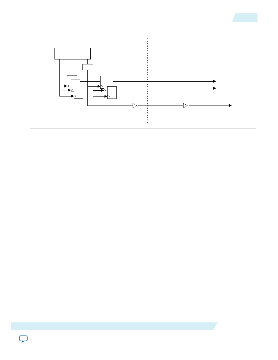
Figure 8: ALTLVDS_RX Block in No Output Register Mode
DPA
ALTLVDS_RX
Core
ALTLVDS_RX
fast registers
ALTLVDS_RX
slow registers
divfwdclk
÷
rx_out[]
rx_divfwdclk
DPA PLL Calibration
The following sections describe DPA PLL calibration and its effects in Stratix III, Stratix IV,
Stratix IV Engineering Sample (ES), and Arria II devices.
•
DPA PLL Calibration in Stratix IV ES Devices
•
DPA PLL Calibration in Arria II and Stratix IV Devices and Later
•
Effects of DPA PLL Calibration
on page 51
Related Information
DPA PLL Calibration in Stratix IV ES Devices
Applications using a fixed, cyclical training pattern with sparse data transitions can cause the PLL phase
to remain unchanged, which results in DPA misalignment. When DPA misaligns the DPA circuitry
remains at the initial configured phase or takes a significantly longer time to lock onto the optimum
phase. A non-ideal phase might result in data bit errors, even after the DPA lock signal goes high.
Resetting the DPA circuit may not solve the problem.
The following figure shows that the DPA takes longer time to lock onto the optimum phase even after the
rx_reset
and
rx_dpa_locked
signals are asserted, resulting in data errors.
UG-MF9504
2014.12.15
DPA PLL Calibration
49
LVDS SERDES Transmitter/Receiver IP Cores User Guide
Altera Corporation