Altera LVDS SERDES Transmitter / Receiver User Manual
Page 56
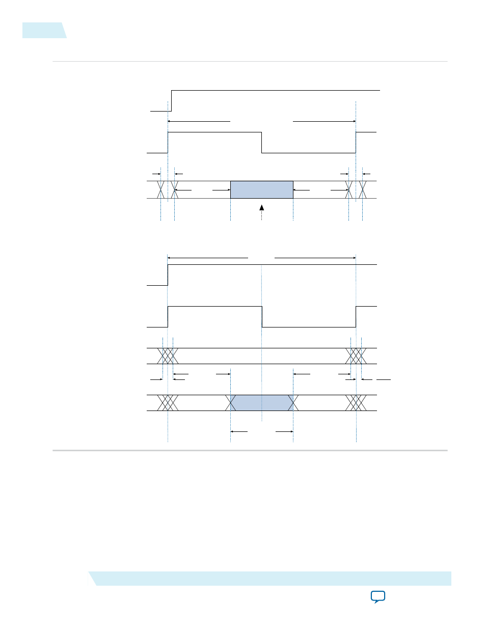
Figure 11: Differential High-Speed Timing Diagram and Timing Budget for Non-DPA Mode
TUI
RCCS
RCCS
SW
RCCS
RSKM
RSKM
SW
RSKM
RSKM
External
Input Clock
Internal
Clock
Receiver
Input Data
Timing Budget
External
Clock
Internal
Clock
Synchronization
Transmitter
Output Data
Receiver
Input Data
Timing Diagram
Time Unit Interval (TUI)
t
SW
(min)
Bit n
t
SW
(max)
Bit n
Internal
Clock
Falling Edge
Clock Placement
RCCS
2
You must calculate the RSKM value to decide whether you can properly sample the data by the LVDS
receiver with the given data rate and device. A positive RSKM value indicates the LVDS receiver can
properly sample the data; a negative RSKM value indicates the receiver cannot properly sample the data.
The following example shows the RSKM calculation.
Data Rate: 1 Gbps, Board channel-to-channel skew = 200 ps
56
Receiver Skew Margin and Transmitter Channel-to-Channel Skew
UG-MF9504
2014.12.15
Altera Corporation
LVDS SERDES Transmitter/Receiver IP Cores User Guide