Altera LVDS SERDES Transmitter / Receiver User Manual
Page 60
set_input_delay -clock [get_clocks virtual_clock_lvds] -clock_fall -max
0.200 [get_ports rx_in*] -add_delay
set_input_delay -clock [get_clocks virtual_clock_lvds] -clock_fall -min
-0.200 [get_ports rx_in*] -add_delay
To add the .sdc into your Quartus II design file, follow these steps:
1. In the Quartus II software, click on the Assignments menu, and select Settings.
2. On the Settings page, under Category, select TimeQuest Timing Analyzer.
3. On the TimeQuest Timing Analyzer subwindow, browse to the .sdc, and click Add.
4. Click OK.
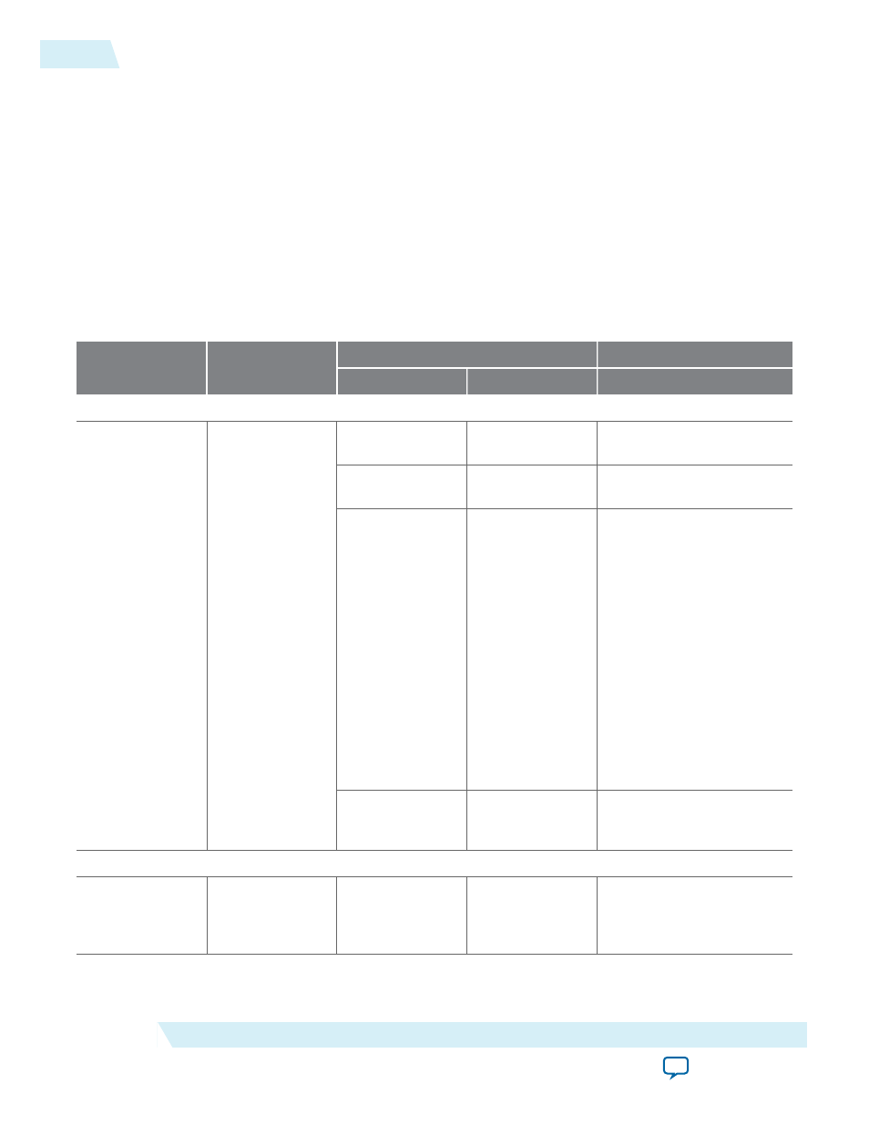
The following table lists the LVDS timing constraints options and descriptions.
Table 12: LVDS Timing Constraints Options and Descriptions
Port Name
Constraint Type
Option
Description
GUI Setting
SDC command
Input Clock Constraints
rx_inclock
create_clock
Clock name
-name
Specifies the name of the
LVDS input clock.
Period
-period
Specifies the clock period
(1/f
max
).
Rising, Falling
-waveform
Specifies the clock's rising
and falling edges or the
duty cycle of the clock.
For example, a 10 ns
period where the first
rising edge occurs at 0 ns
and the first falling edge
occurs at 5 ns would be
written as waveform {0 5}.
The difference must be
within one period unit,
and the rise edge must
come before the fall edge.
The default edge list is {0
<period>/2}, or a 50
percent duty cycle.
Target
[get_ports
{<port
name>}
]
Specifies the clock input
port name connected to
rx_inclock
.
Synchronous Input Port Constraints
Minimum,
Maximum
-max
-min
Specifies the maximum
and minimum delay for
the data input to the
FPGA.
60
Setting Timing Constraints Manually in the Synopsys Design Constraint File
UG-MF9504
2014.12.15
Altera Corporation
LVDS SERDES Transmitter/Receiver IP Cores User Guide