Altera LVDS SERDES Transmitter / Receiver User Manual
Page 63
From the PLL
To the ALTLVDS Transmitter
To the ALTLVDS Receiver
Load enable output (c1)
tx_enable
(load enable to the
transmitter)
rx_enable
(load enable for the deserializer)
Parallel clock output (c2)
Parallel clock used inside the
transmitter core logic in the
FPGA fabric
rx_syncclock
(parallel clock input) and
parallel clock used inside the receiver core
logic in the FPGA fabric
~(locked)
—
pll_areset
(asynchronous PLL reset port)
Note: The
pll_areset
signal is
automatically enabled for the
LVDS receiver in external PLL
mode. This signal does not exist
for LVDS transmitter instantia‐
tion when the external PLL
option is enabled.
The
rx_syncclock
port is not always required by the LVDS receiver in external PLL mode. If it is
required, the Quartus II software automatically generates the port. Even if
rx_syncclock
(c2) is not used
in the LVDS receiver, you must still use it to clock the FPGA fabric. The Quartus II compiler errors out if
this port is not connected, as shown in the following figure.
Note: When generating the ALTPLL IP core for Arria II devices, select the Left/Right PLL PLL type to
set up the PLL for LVDS.
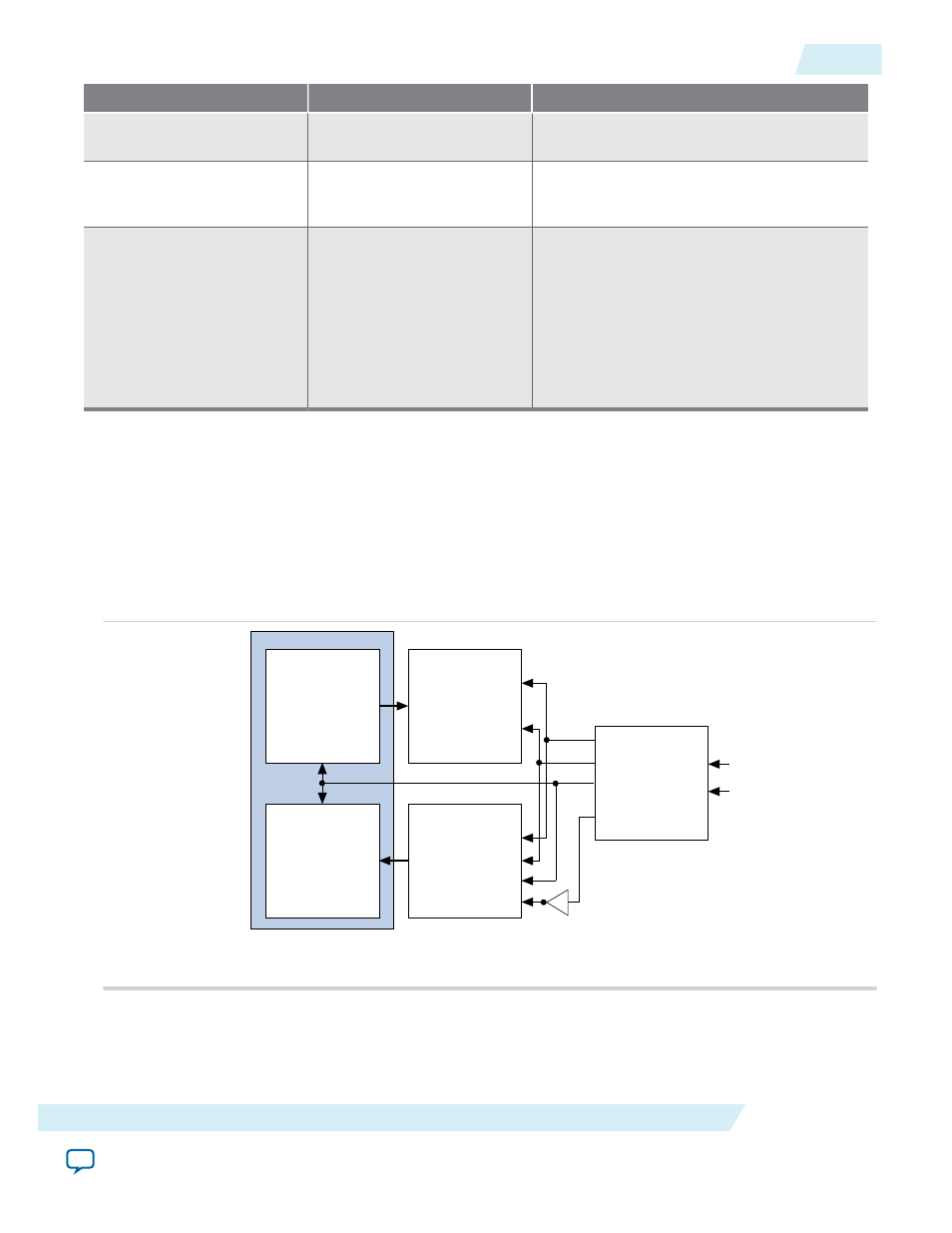
The following figure shows the connection between the PLL IP core and the ALTLVDS IP core.
Figure 14: LVDS Interface with the PLL IP Core
tx_coreclk
tx_in
FPGA Fabric
c0
inclk0
c1
c2
rx_out
pll_areset
Instantiation of pll_areset is optional for the ALTPLL instantiation.
LVDS Transmitter
(ALTLVDS)
LVDS Receiver
(ALTLVDS) rx_inclock
rx_enable
rx_syncclock
pll_areset
Receiver Core Logic
Transmitter Core Logic
rx_coreclk
ALTPLL
tx_inclock
tx_enable
locked
UG-MF9504
2014.12.15
PLL Clock Signals for LVDS Interface in External PLL Mode
63
LVDS SERDES Transmitter/Receiver IP Cores User Guide
Altera Corporation