Altera LVDS SERDES Transmitter / Receiver User Manual
Page 64
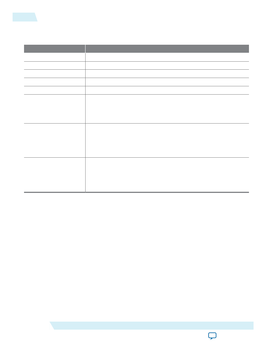
Table 14: Example Settings to Generate Three Output Clocks using PLL IP Core
This table shows an example with the parameter values that you can set in the PLL IP core parameter editor to
generate three output clocks.
Parameter/Clock
Setting
Serial clock
Frequency = 1000 MHz
Parallel clock
Frequency = 100 MHz (serial clock divided by the serialization factor)
LVDS data rate
1 Gbps
Serialization factor
10
Input reference clock
Frequency = 100 MHz
c0
• Frequency = 1000 MHz (multiplication factor = 10 and division factor = 1)
• Phase shift = –180° with respect to the voltage-controlled oscillator (VCO)
clock
• Duty cycle = 50%
c1
• Frequency = (1000/10) = 100 MHz (multiplication factor = 1 and division
factor = 1)
• Phase shift = (10 - 2) × 360/10 = 288° [(deserialization factor - 2)/deseriali‐
zation factor] × 360°
• Duty cycle = (100/10) = 10% (100 divided by the serialization factor)
c2
• Frequency = (1000/10) = 100 MHz (multiplication factor = 1 and division
factor = 1)
• Phase shift = (–180/10) = –18° (c0 phase shift divided by the serialization
factor)
• Duty cycle = 50%
Phase shift calculations using RSKM equation assume that the input clock and serial data are edge aligned.
The following figure shows that by introducing a phase shift of –180° to sampling clock (c0) ensures that
the input data is center-aligned with respect to the
c0
.
Note: The phase shift example used in this section assumes that the clock and data are edge-aligned at the
FPGA pins. For other clock relationships, Altera recommends that you create the ALTLVDS_TX
and ALTLVDS_RX IP cores initially without using the external PLL option. Set the phase shifts you
require in the parameter editor and then note the phase shift and duty cycle settings for the three
PLL output clocks in the Quartus II software Compilation Report (Resource > Fitter > PLL Usage
section). Once you have the correct phase shift and duty cycle settings for your parameterization,
you can implement the external PLL mode in your design. In the parameter editor for the PLL IP
core, enter the phase shift and duty cycle values for each output clock based on the values you
previously noted from the PLL Usage report.
64
PLL Clock Signals for LVDS Interface in External PLL Mode
UG-MF9504
2014.12.15
Altera Corporation
LVDS SERDES Transmitter/Receiver IP Cores User Guide