Fluke Biomedical 956A-201-M2 User Manual
Page 46
3-20
3.13 FUNCTIONAL DESCRIPTION, MODEL 897A G-M
DETECTOR
897A Series Detector
Functionally, the detector is divided into the G-M tube and the preamplifier. The high voltage power supply
for the detector is located in the 956A-201-M2 Universal Digital Ratemeter. The block diagram for the
897A Series Detectors is shown in Figure 3-1. For additional information, refer to the applicable drawings
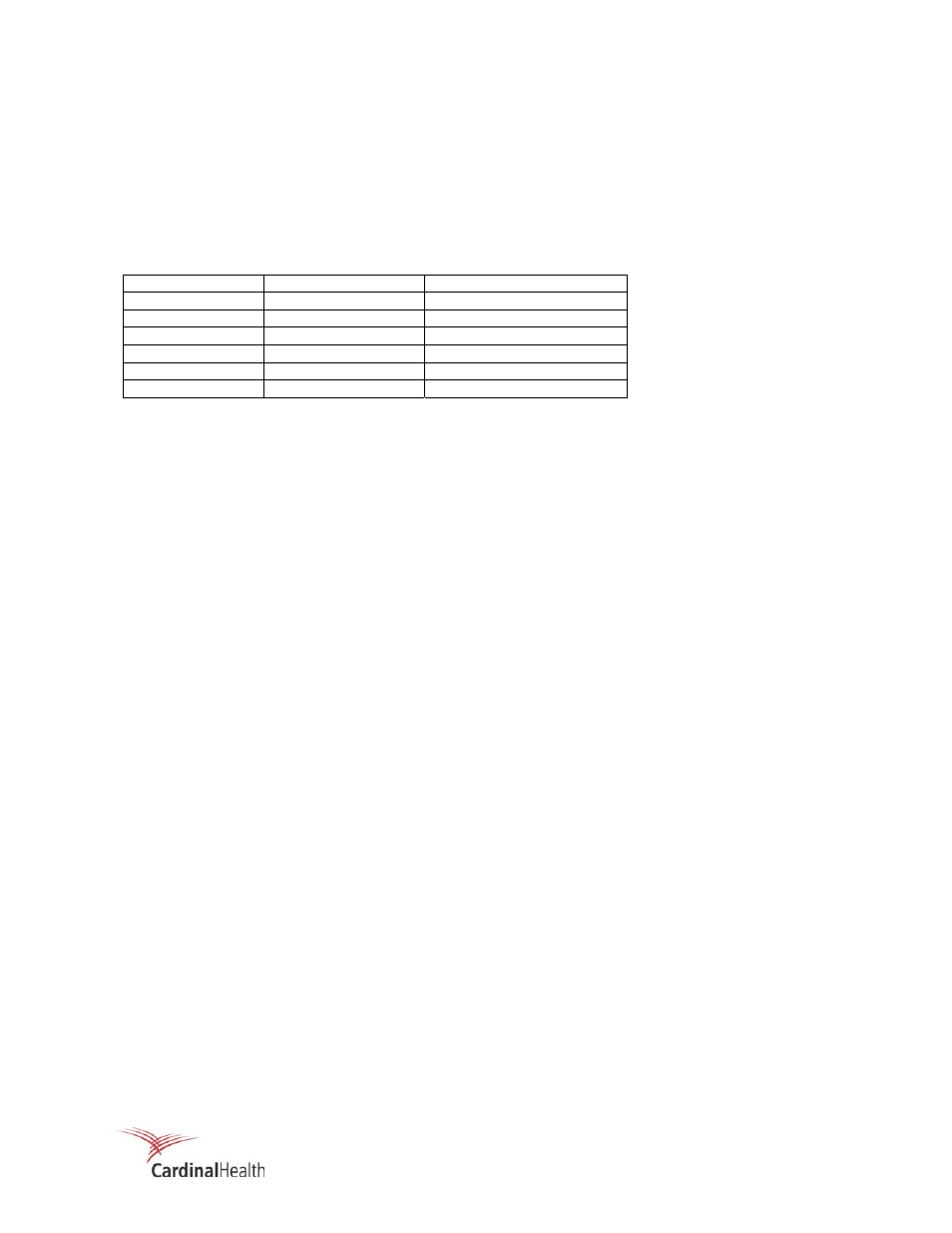
located in Appendix B. The following versions of the Model 897A detector are available:
Model Number
Range
Material
897A-210
0.01 to 1.00E3 mR/h Carbon Steel Housing
897A-211
0.01 to 1.00E3 mR/h Stainless Steel Housing
897A-220
0.10 to 1.00E4 mR/h Carbon Steel Housing
897A-221
0.10 to 1.00E4 mR/h Stainless Steel Housing
897A-230
1.00 to 1.00E5 mR/h Carbon Steel Housing
897A-231
1.00 to 1.00E5 mR/h Stainless Steel Housing
The 897A Series detector is a thin walled, electronic tube composed of a negative electrode (cathode) and
a positive electrode (anode). The tube is filled with a mixture of one or more noble gases, plus a small
amount of an additional gas that acts as a quenching agent.
Circuit Description
Quad comparator Z1 consists of two (2) circuit configurations with four states. Three of the four states are
comparators (Z1A is an input comparator, Z1B is an output comparator, and Z1C is an anti-jam
comparator). The fourth state, Z1D, is an oscillator for the anti-jam circuitry.
Transistors Q3 and Q4, with associated circuitry, provide a divide by 2 function, for use with Victoreen
analog and digital area monitor readouts.
When ionizing radiation is not present at the G-M detector, the input level of Z1A (pin 9) is higher in
potential than the voltage level at pin 8. Using discriminator bias control R44, the amount of potential
difference can be adjusted between these inputs, allowing input pulse discrimination. Under the above
condition, the output of Z1A is in a high state. R23, R20, and R30 create a voltage divider that biases pin
7 of Z1B to 7.5 Vdc. R24 and R36 bias pin 6 to 5 Vdc, causing the output of Z1B to go high. This action
allows Q1 to conduct, causing a low state to exist at the output.
When an ionizing event occurs, the G-M tube produces a negative pulse that is coupled through C10 to
input comparator Z1A. Pin 9 is now at a lower voltage potential than pin 8 forcing the output of Z1A to a
low state. The voltage at pin 7 of Z1B is reduced to 2.5 Vdc, causing a low output state. This action
causes Q2 to conduct, presenting a +10 Vdc signal at the output (unterminated).
If saturation occurs, the detector provides a high dc current. The current flows through R25, inducing a
voltage at pin 11 of Z1C. When the potential at Z1C is higher than the anti-jam setpoint (R41), the output
is forced from a low state (normal operating condition) to a high state. Two (2) events occur when a
saturation condition exists:
1. Q5, normally off, enters saturation, clamping the output of Z1A to a low state. The potential at pin 5 of
Z1D is reduced to 2.5 Vdc.
2. CR6 is reverse biased, enabling anti-jam oscillator Z1D. A square wave pulse of approximately
40,000 Hz is produced at pin 6 of Z1B that has an amplitude that is approximately 5.0 Vdc. Since pin
7 was previously biased to 2.5 Vdc, an output anti-jam square wave signal is generated and coupled
to the readout.