Fluke Biomedical 956A-201-M2 User Manual
Page 54
3-28
5. If programs are not executed from on-board RAM,
t
AV1 applies. If programs are to be stored and
executed from on-board RAM,
t
AV2 applies. For normal data storage in the on-board RAM, this
extended delay does not apply. Programs cannot be executed from on-board RAM when using A and
B parts (MC68A02, MC68A08, MC68B02, MC68B08). ON-board RAM can be used for data storage
with all parts.
Reset Circuitry
The reset circuit generates a 650 ms wide low pulse to the MPU reset input and various external registers.
The R1/C1 network generates a delayed trigger pulse to the U10 multivibrator. Upon power up, C1
charges through R1. When approximately 1.4 volts are reached, U11-8 goes low, triggering U10. U10-4
goes low, U10-13 goes high; this condition is held for 650 ms. When U10's delay is complete, U10-4
returns high and U10-13 returns low. The low to high transition on U10-4 signals the MPU to begin a reset
sequence. JP1 - Reset Pins, on the circuit board, may be shorted to initiate an MPU reset for
troubleshooting purposes.
Clocks
The system clock is generated by the MPU using a 4 MHz crystal, CR1. The system clock, from which
others are derived, is an output on the MPU pin 37 and operates at 1 MHz.
NMI Clock
The NMI clock is generated by U30, U31, and U32, which are dual decade counters. The 1 MHz system
clock is applied to the U30-1 input. U30 is a divide by 100 counter, while U31 is a divide by 50 counter,
with respect to the input frequency. Therefore, U30-9's output is 10 kHz and U31-9's output is 200 Hz.
U32 is connected for operation as a divide by 25 counter, which produces an 8 Hz output on U32-9.
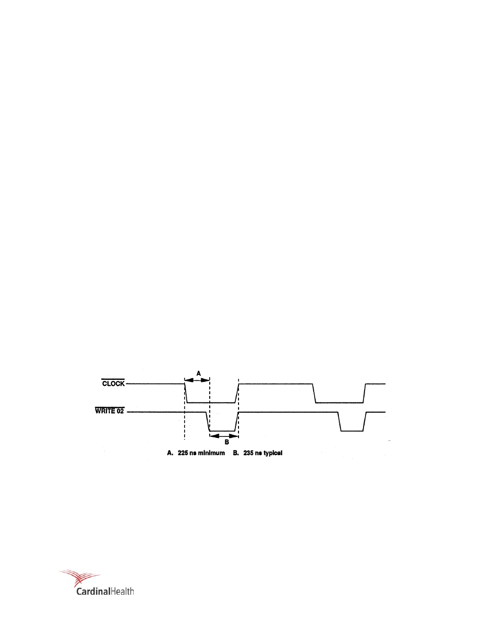
Write Cycle Clock
The Write Cycle Clock is generated by U19. The 1 MHz system clock is applied to the U19A-2 input,
which is adjusted via VR 13 for a -225 ns delay from the falling clock edge. The second stage of U19,
U19B produces a 225 ns output pulse width. Figure 3-5 is the timing diagram for the write cycle clock.
Signals SHORT02 and /SHORT02 are buffered by U18 to produce WRITE02 and /WRITE02 that are used
by the system.
Table 3-5. Write Cycle Clock Timing Diagram
Address Drivers
Line drivers U12 (low order addresses) and U13 (high order addresses) provide signal buffering and
capability to drive 15 TTL’s unit loads for the address bus. The output drives are all internal devices
utilizing address signals on the main circuit board as well as the J3 option interface bus connector for
additional circuit boards.